
OSPI
Introduction
Octal Serial Peripheral Interface (OSPI) is an extended Serial Peripheral Interface (SPI) protocol. Compared with standard SPI, OSPI shares 8 data lines for transmitting and receiving. The communication mode is synchronous half-duplex. In the GR5526 SoC, the OSPI interface is only used to connect the PSRAM device supporting XccelaBus.
This module is only existed in graphics enhanced chips.
Main Features
Main features of the OSPI modules include:
- OSPI.DDR-PSRAM solution (Octal SPI with DDR Xccela mode, two bytes transferred per one clock cycle)
- 64 Mb 1.8V PSRAM (8 M x 8 bits with 1024 bytes page size)
- 48 MHz memory access frequency
- Variable latency and constant latency
- Adjustable drive strength
- Active mode, half-sleep mode, and deep power down
- Support for DMA (limited to aligned address)
- Support for global reset (using command instructions)
Functional Description
Block Diagram

The OSPI AHB-Lite memory controller has two system-side interfaces, namely APB and AHB-Lite interfaces.
The APB interface is used to access the control and status register (CSR) inside the controller. The AHB-Lite interface is used to write/read memory arrays and write/read mode registers in AP storage devices based on CSR register settings.
The AP_MEM_CNTR_IP instance is the digital controller IP. The OPI_PHY is responsible for generating AP memory interface signals and handling part of the timing maintenance together with the controller.
Control Interface
The commands specified on the INST (Instruction) cycle defined by the Address/DQ pins are latched on the first rising edge of the clock. The sampling address is latched on the rising/falling edge of the second or third clock. After address latching, the device initializes Data Strobe (DQS)/Data Mask (DM) to 0 from next CLK rising edge of the third clock cycle.
Output data is available after LC latency cycles. In case of internal refresh insertion, variable latency output data may be delayed by up to (LC*2) latency cycles. True variable refresh pushout latency can be anywhere between LC to LCx2. The first DQS/DM rising edge after reading the preamble indicates the beginning of valid data.
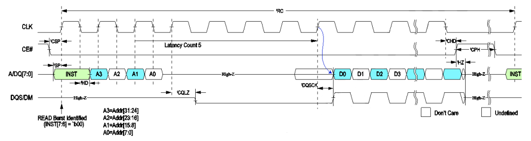
Extra payload may exist in reading. Due to the complexity of Xccela control, the master logic cannot switch the state in time after reading the expected data, causing the slave to continue to generate unexpected data. Because this part of the data is not considered as the payload, it will reduce the access efficiency. Using MCU to access OSPI in reading will generate more extra DQS clocks than using DMA/GPU. Excessive overhead will reduce access efficiency. The access mode of MCU under Cortex®-M4F is INCR. Bursts will affect the access efficiency so that the practice of using MCU to access OSPI in reading should be minimized.
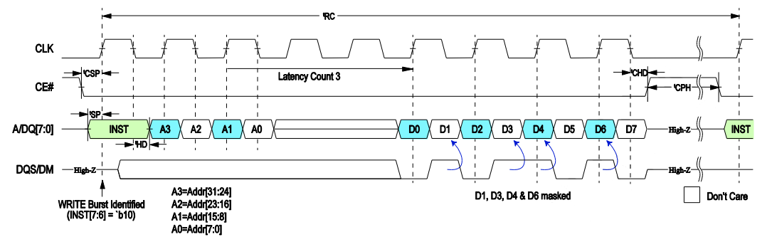
At least 2 bytes of data must be input in the write operation. In the case of continuous short burst writes, tRC must be met by issuing additional CE# high time between operations. Single-byte write operations can be performed by using DQS/DM to mask unwritten bytes.
It is worth noting that PSRAM has been embedded in GR5526, but it needs to be enabled before using OSPI controller. By default, the PSRAM is disabled considering the impact of power consumption of PSRAM. The impedance matching between OSPI controller and PSRAM can be modified by adjusting the drive strength of PSRAM. Lower drive strength indicates lower power consumption. The waveform tends to be triangle wave, and the quality of the waveform is worse. Greater drive strength indicates higher power consumption. The waveform tends to be square wave, and the quality of the waveform is better. However, excessive drive strength may lead to system crash. Therefore, an appropriate drive strength should be selected according to the application scenario.
Registers
MEM_BASE_ADDR
- Name: Bottom/Base Memory Address Register
- Description: This register represents the bottom/base address of the memory.
- Base Address: 0x40024000
- Offset: 0x0
- Reset Value: 0x00000000
| Bits | Field Name | RW | Reset | Description |
|---|---|---|---|---|
31:25 |
RSVD |
R |
Reserved bits |
|
24:0 |
MEM_BASE_ADDR |
RW |
0x0 |
This represents the bottom/base address of the memory. Note: This reset value is for the bottom array of a memory. |
MEM_TOP_ADDR
- Name: Top Memory Address Register
- Description: This register represents the top address of the memory.
- Base Address: 0x40024000
- Offset: 0x4
- Reset Value: 0x01FFFFFF
| Bits | Field Name | RW | Reset | Description |
|---|---|---|---|---|
31:25 |
RSVD |
R |
Reserved bits |
|
24:0 |
MEM_TOP_ADDR |
RW |
0x1FFFFFF |
This represents the top address of the memory. Note: This reset value is based on 256 Mb device density memory. |
GLOBAL_RESET
- Name: Global Reset Register
- Description: This register configures global reset.
- Base Address: 0x40024000
- Offset: 0x8
- Reset Value: 0x00000216
| Bits | Field Name | RW | Reset | Description |
|---|---|---|---|---|
31:10 |
RSVD |
R |
Reserved bits |
|
9:1 |
TRST_CNT |
RW |
0x10B |
This holds the CE# high time in terms of mem_clk cycles between reset command execution and subsequent write/read operation. Note: The reset value corresponds to 2 μs at 133 MHz. |
0 |
GLOBAL_RESET_EN |
RW |
0x0 |
1: Enables the global reset instruction to be initiated to the memory. Note: This bit is cleared to zero by itself after this transaction completes with the memory. Users should not write zero to this bit. |
ACCESS_TYPE
- Name: Access Type Register
- Description: This register controls access type.
- Base Address: 0x40024000
- Offset: 0xC
- Reset Value: 0x00000001
| Bits | Field Name | RW | Reset | Description |
|---|---|---|---|---|
31:1 |
RSVD |
R |
Reserved bits |
|
0 |
MR_ACCESS |
RW |
0x1 |
Memory array or mode register access 0: Memory array access 1: Mode register access |
ACCESS_TIMING
- Name: Access Timing Register
- Description: This register sets TCEM, TRC, TCPH timing, and page size.
- Base Address: 0x40024000
- Offset: 0x10
- Reset Value: 0x00A50840
| Bits | Field Name | RW | Reset | Description |
|---|---|---|---|---|
31:25 |
RSVD |
R |
Reserved bits |
|
24 |
EN_EFF_THRGHPUT |
RW |
0x0 |
Enable efficient read throughput. 1: Enhance the read throughput by enabling this bit in CSR, TCEM_TRC_PAGE_SIZE_RD_THRGHPUT_REG [tcem_time_ignore]. This bit should be set to 1 and also the row boundary crossing in the PSRAM memory should be enabled. |
23:20 |
MEM_PAGE_SIZE |
RW |
0xA |
Page size in memory = 2^(mem_page_size)
|
19:17 |
TCPH_CNT |
RW |
0x2 |
This holds the CE# HIGH time in terms of mem_clk cycles between subsequent burst operations in terms of mem_clk cycles. Note: The reset value corresponds to 15 ns at 133 MHz. |
16:13 |
TRC_CNT |
RW |
0x8 |
This holds the write and read cycle time (tRC) in terms of mem_clk cycles. Note: The reset value corresponds to 60 ns at 133 MHz. |
12:1 |
TCEM_CNT |
RW |
0x420 |
This is the CE# low pulse width time in terms of mem_clk cycles, during any memory array access. The default value is set based on 133 MHz memory clock operation. |
0 |
TCEM_TIME_IGNORE |
RW |
0x0 |
1: If tCEM time needs not be taken care by the controller, then F/W shall set this bit. Note: This bit should be set to 1 during WRAP transfers. |
DEEP_DOWN_CTRL
- Name: Deep Down Control Register
- Description: This register controls deep power down.
- Base Address: 0x40024000
- Offset: 0x14
- Reset Value: 0x00427100
| Bits | Field Name | RW | Reset | Description |
|---|---|---|---|---|
31:23 |
RSVD |
R |
Reserved bits |
|
22:19 |
DPD_EXIT_CYCLE_CNT |
RW |
0x8 |
This decides the tXPDPD time during deep power down exit. In multiples of mem_clk cycles (Min value of 60 ns). The default value is set based on 133 MHz memory clock operation and tXPDPD time 60 ns. |
18:3 |
TXDPD_COUNT |
RW |
0x4E20 |
This decides the tXDPD time during deep power down exit in terms of mem_clk cycles. The default value is set based on 133MHz memory clock operation and tXDPD time 150 μs. |
2 |
TXDPD_TIME_IGNORE |
RW |
0x0 |
1: If F/W can take care of the tXDPD time, it can set this bit. By setting this bit, the controller shall not run an internal counter (based on mem_clk) to take care of the tXDPD time. Hence, the system can shut off the mem_clk to the controller. |
1 |
DPD_EXIT |
RW |
0x0 |
1: Triggers the deep power down exit instruction to be sent to the memory. Note: This bit is cleared to zero by itself after this transaction completes with the memory. Users should not write zero to this bit. |
0 |
DPD_ENTRY |
RW |
0x0 |
1: Triggers the deep power down entry instruction to be sent to the memory. Note: This bit is cleared to zero by itself after this transaction completes with the memory. Users should not write zero to this bit. |
HALF_SLP_CTRL
- Name: Half Sleep Control Register
- Description: This register controls half sleep.
- Base Address: 0x40024000
- Offset: 0x18
- Reset Value: 0x0041A0B0
| Bits | Field Name | RW | Reset | Description |
|---|---|---|---|---|
31:22 |
RSVD |
R |
Reserved bits |
|
21:18 |
HS_EXIT_CYCLE_CNT |
RW |
0x8 |
This decides the tXPHS time during half-sleep exit. In multiples of mem_clk cycles (min value of 60 ns). The default value is set based on 133 MHz memory clock operation and tXPHS time 60 ns |
17:3 |
TXHS_COUNT |
RW |
0x3416 |
This decides the tXHS time during half sleep exit in terms of mem_clk cycles. The default value is set based on 133 MHz memory clock operation and tXHS time 100 μs. |
2 |
TXHS_TIME_IGNORE |
RW |
0x0 |
1: If F/W can take care of the tXHS time, it can set this bit. By setting this bit, the controller shall not run an internal counter (based on mem_clk) to take care of the tXHS time. Hence, the system can shut off the mem_clk to the controller. |
1 |
HS_EXIT |
RW |
0x0 |
1: Triggers the Half sleep exit instruction to be sent to the memory. Note: This bit is cleared to zero by itself after this transaction completes with the memory. Users should not write zero to this bit. |
0 |
HS_ENTRY |
RW |
0x0 |
1: Triggers the Half sleep entry instruction to be sent to the memory. Note: This bit is cleared to zero by itself after this transaction completes with the memory. Users should not write zero to this bit. |
INT_CTRL
- Name: Interrupt Control Register
- Description: This register controls interrupt kinds.
- Base Address: 0x40024000
- Offset: 0x1C
- Reset Value: 0x00000000
| Bits | Field Name | RW | Reset | Description |
|---|---|---|---|---|
31:6 |
RSVD |
R |
Reserved bits |
|
5 |
DQS_TIMEOUT_IE |
RW |
0x0 |
1: Generates an interrupt when DQS timeout occurs during read operation. |
4 |
DPD_EXIT_IE |
RW |
0x0 |
1: Generates an interrupt when deep power down exit transfer to the AP memory device completes. |
3 |
DPD_ENTRY_IE |
RW |
0x0 |
1: Generates an interrupt when deep power down entry transfer to the AP memory device completes. |
2 |
HS_EXIT_IE |
RW |
0x0 |
1: Generates an interrupt when half-sleep exit transfer to the AP memory device completes. |
1 |
HS_ENTRY_IE |
RW |
0x0 |
1: Generates an interrupt when half-sleep entry transfer to the AP memory device completes. |
0 |
GLOBAL_RESET_IE |
RW |
0x0 |
1: Generates an interrupt when global reset transfer to the AP memory device completes. |
XFER_STAT
- Name: Transfer Status Register
- Description: This register shows transfer status.
- Base Address: 0x40024000
- Offset: 0x20
- Reset Value: 0x00000000
| Bits | Field Name | RW | Reset | Description |
|---|---|---|---|---|
31:6 |
RSVD |
R |
Reserved bits |
|
5 |
DQS_NON_TOGGLE_ERR |
RC |
0x0 |
This bit is set if “DQS” from the memory is not toggling during AHB-Lite initiated memory read/mode register read operation. |
4 |
DPD_EXIT_DONE |
RC |
0x0 |
This bit is set to denote that the APB-CSR initiated deep power down exit transfer completes. |
3 |
DPD_ENTRY_DONE |
RC |
0x0 |
This bit is set to denote that the APB-CSR initiated deep power down entry transfer completes. |
2 |
HS_EXIT_DONE |
RC |
0x0 |
This bit is set to denote that the APB-CSR initiated half sleep exit transfer completes. |
1 |
HS_ENTRY_DONE |
RC |
0x0 |
This bit is set to denote that the APB-CSR initiated entry transfer completes. |
0 |
GLOBAL_RESET_DONE |
RC |
0x0 |
This bit is set to denote that the APB-CSR initiated global reset transfer completes. |
CMD_CTRL_1
- Name: Command Control Register 1
- Description: This register is command control register.
- Base Address: 0x40024000
- Offset: 0x24
- Reset Value: 0xA0208000
| Bits | Field Name | RW | Reset | Description |
|---|---|---|---|---|
31:24 |
LINEAR_BURST_WR |
RW |
0xA0 |
This holds the command to be sent to the memory during linear burst write operation. |
23:16 |
LINEAR_BURST_RD |
RW |
0x20 |
This holds the command to be sent to the memory during linear burst read operation. |
15:8 |
SYNC_WR |
RW |
0x80 |
This holds the command to be sent to the memory during sync write operation |
7:0 |
SYNC_RD |
RW |
0x0 |
This holds the command to be sent to the memory sync read operation. |
CMD_CTRL_2
- Name: Command Control Register 2
- Description: This register is command control register.
- Base Address: 0x40024000
- Offset: 0x28
- Reset Value: 0x00FFC040
| Bits | Field Name | RW | Reset | Description |
|---|---|---|---|---|
31:24 |
RSVD |
R |
Reserved bits |
|
23:16 |
GLOBAL_RESET_CMD |
RW |
0xFF |
This holds the command to be sent to the memory during global reset operation. |
15:8 |
MODE_REG_WR |
RW |
0xC0 |
This holds the command to be sent to the memory during mode register write operation. |
7:0 |
MODE_REG_RD |
RW |
0x40 |
This holds the command to be sent to the memory during mode register read operation. |
DQS_TIMEOUT
- Name: DQS Timeout Register
- Description: This register sets DQS timeout.
- Base Address: 0x40024000
- Offset: 0x2C
- Reset Value: 0x00000000
| Bits | Field Name | RW | Reset | Description |
|---|---|---|---|---|
31:5 |
RSVD |
R |
Reserved bits |
|
4:0 |
DQS_NON_TGL_TIMEOUT |
RW |
0x0 |
Read DQS non-toggling timeout. This is to set the tRBXwait (as per spec.) This holds the maximum number of mem_clk cycles for which the controller has to wait for the DQS toggling during row boundary crossing in a read operation. |
PHY_CTRL_0
- Name: PHY Control Register 0
- Description: This register controls PHY.
- Base Address: 0x40024000
- Offset: 0x30
- Reset Value: 0x00000000
| Bits | Field Name | RW | Reset | Description |
|---|---|---|---|---|
31:0 |
PHY_CNTRL_REG0 |
RW |
0x0 |
PHY control register 0 |
PHY_CTRL_1
- Name: PHY Control Register 1
- Description: This register controls PHY.
- Base Address: 0x40024000
- Offset: 0x34
- Reset Value: 0x00000000
| Bits | Field Name | RW | Reset | Description |
|---|---|---|---|---|
31:0 |
PHY_CNTRL_REG1 |
RW |
0x0 |
PHY control register 1 |
PHY_CTRL_2
- Name: PHY Control Register 2
- Description: This register controls PHY.
- Base Address: 0x40024000
- Offset: 0x38
- Reset Value: 0x00000000
| Bits | Field Name | RW | Reset | Description |
|---|---|---|---|---|
31:0 |
PHY_CNTRL_REG2 |
RW |
0x0 |
PHY control register 2 |
PHY_CTRL_3
- Name: PHY Control Register 3
- Description: This register controls PHY.
- Base Address: 0x40024000
- Offset: 0x3C
- Reset Value: 0x00000000
| Bits | Field Name | RW | Reset | Description |
|---|---|---|---|---|
31:0 |
PHY_CNTRL_REG3 |
RW |
0x0 |
PHY control register 3 |
PHY_CTRL_4
- Name: PHY Control Register 4
- Description: This register controls PHY.
- Base Address: 0x40024000
- Offset: 0x40
- Reset Value: 0x00000000
| Bits | Field Name | RW | Reset | Description |
|---|---|---|---|---|
31:0 |
PHY_CNTRL_REG4 |
RW |
0x0 |
PHY control register 4 |
PHY_CTRL_5
- Name: PHY Control Register 5
- Description: This register controls PHY.
- Base Address: 0x40024000
- Offset: 0x44
- Reset Value: 0x00000000
| Bits | Field Name | RW | Reset | Description |
|---|---|---|---|---|
31:0 |
PHY_CNTRL_REG5 |
RW |
0x0 |
PHY control register 5 |
PHY_CTRL_6
- Name: PHY Control Register 6
- Description: This register controls PHY.
- Base Address: 0x40024000
- Offset: 0x48
- Reset Value: 0x00000000
| Bits | Field Name | RW | Reset | Description |
|---|---|---|---|---|
31:0 |
PHY_CNTRL_REG6 |
RW |
0x0 |
PHY control register 6 |
PHY_CTRL_7
- Name: PHY Control Register 7
- Description: This register controls PHY.
- Base Address: 0x40024000
- Offset: 0x4C
- Reset Value: 0x00000000
| Bits | Field Name | RW | Reset | Description |
|---|---|---|---|---|
31:0 |
PHY_CNTRL_REG7 |
RW |
0x0 |
PHY control register 7 |
RD_PREFETCH
- Name: Read Prefetch Register
- Description: This register controls read prefetch.
- Base Address: 0x40024000
- Offset: 0x50
- Reset Value: 0x00000000
| Bits | Field Name | RW | Reset | Description |
|---|---|---|---|---|
31:1 |
RSVD |
R |
Reserved bits |
|
0 |
RD_PREFETCH_EN |
RW |
0x0 |
1: Read data pre-fetch is enabled in the controller for read operation. 0: Read data prefetch is disabled in the controller for read operation. |
