
GPU
Introduction
Graphics Processing Unit (GPU) is a kind of microprocessor that specializes in image and graphic related operations. GR5526 integrates a low-power GPU which can bring high-quality graphics to the user interface with a very small silicon/power budget. It supports entry-level IoT platforms, wearables, and embedded devices with low-cost and ultra-low power consumption requirements, and provides a smooth graphical experience suitable for various applications. Developers can create compelling graphical user interfaces (GUIs) and software applications with extremely long battery life for power-memory-area constrained IoT devices at significantly lower cost.
Main Features
- Hardware components:
- Programmable shader engine with a very long instruction word (VLIW) architecture
- Command-list-based DMAs to minimize CPU overhead
- Primitive rasterizer
- Texture mapping unit
- Blending unit
- Drawing primitives:
- Pixel/Line drawing
- Filled rectangles
- Triangles (Gouraud shaded)
- Quadrilaterals
- Color formats:
- 32-bit RGBA8888/BGRA8888/ABGR8888
- 24-bit RGB
- 16-bit RGBA5551/RGB565
- 8-bit A8/L8/RGB332
- TSCTM
- Compression & Decompression feature:
- Image transformation
- Texture mapping
- Point sampling
- Bilinear filtering
- Blit support
- Rotation any angle
- Mirroring
- Stretch (independently on X and Y axes)
- Source and/or destination color keying
- Format conversions on the fly
- 2.5D perspective correct projections
- Text rendering support:
- Bitmap antialiased A1/A2/A4/A8
- Font Kerning
- Unicode (UTF8)
- Blending support:
- Fully programmable Alpha blending modes (source and destination)
- Source/Destination color keying
- Antialiasing:
- 8 x MSAA
- Quadrilaterals per edge antialiasing
- Triangles per edge antialiasing
- Antialiased thick lines
- Antialiased circles
Functional Description
Block Diagram

The fixed-point data path and instruction set architecture (ISA) of the GPU are tailored specifically for GUIs acceleration and small display applications, resulting in significant improvements in power consumption and silicon area. The GPU combines hardware-level support for multithreading, VLIW, and low-level vector processing in the most energy-efficient way. The GPU block diagram is shown above.
I/O Interfaces
The GPU supports connection via AHB that helps it communicate with the MCU, configuration registers, and system memory. The GPU uses two 32-bit AHB master ports that enable access to the main memory and that support data fetch from the G PU (such as textures and frame data). The AHB version of the system fetches both the command lists and rendering data over the same read bus.
Configuration Register File
The GPU is programmed through a set of registers which are known as configuration register file (CRF), and each sub-module of the GPU is programmed through a subset of the CRF. CRF can be memory-mapped to the CPU address space, making it directly accessible. Writing CRF directly is considered inefficient because it consumes a lot of CPU resources and associates CPU execution with the GPU. Therefore, the GPU supports indirect CRF access through the Command List Processor (CLP).
Command List Processor
In order to decouple CPU from GPU execution and achieve both better performance and lower power consumption, the GPU incorporates an advanced Command List Processor (CLP), capable of reading entire lists of commands from the main memory and relaying them to the CRF.
The CPU pre-assembles Command Lists (CLs) prior to submitting them to the CLP for execution, while a single CL can be submitted multiple times. This approach alleviates the CPU from recalculating drawing operations for repetitive tasks, resulting in more efficient resource utilization.
The steps for writing commands to the configuration registers through the CLP are the following:
- The CPU assembles a CL, through the GFX library.
- The CPU submits the CL for execution. The CLP is informed of a pending CL.
- The CLP reads the CL from the system memory.
- The CLP relays the commands to the Configuration Register File.
Rasterizer
The GPU can draw a multitude of geometrical shapes called Geometric Primitives, such as lines, rectangles, triangles, and quadrilaterals. The rasterizer unit reads the coordinates of the primitives’ vertices and feeds the rest of the graphics pipeline with the fragments contained in the geometry. A fragment contains information concerning a single pixel. This information includes raster position (coordinates), texture coordinates, interpolated color, and alpha values.
The rasterizer can draw:
- Line drawing (at any direction)
- Filled rectangles
- Quadrilaterals
- Triangles
In addition, the rasterizer handles clipping by either dropping fragments that are outside the effective drawing area and back-face culling or dropping entire primitives that are considered to be non-visible, like the rear looking faces of a cube. If a pixel resides inside or outside of the geometry primitive, the pixel is determined by the value of E which is positive inside the geometry primitive and negative outside of it.
The pixel’s edge function value is calculated for each line of the geometry primitive (for example, 3 times for a triangle) using the following equation:
Although the equation requires two multiplications and two additions since the variation is always one pixel on the X or Y axis, this is reduced to a single accumulator.
The color variances are also calculated in a similar way, where each of the RGBA components is linearly interpolated across the geometry of the primitive. If H/W Blender is enabled, each edge can be independently programmed to either have antialiasing or not. The rasterizer also determines the coverage value of each pixel as a function of the pixel center to the closest edge distance.
Transformations are performed using matrix multiplication. The Vector Matrix Multiplier multiplies a 2 x 1 Vector (x,y) by a 3 x 3 homogeneous Matrix to produce a new 2 x 1 Vector (Tx,Ty). The following computation is required to calculate texel coordinates from screen coordinates:
Texture Map Unit
The texture map unit produces texels that are sent to the fragment processing core. It is fed with texture’s attributes (base address, dimensions, color format) and the required coordinates. The texture map unit performs some internal processing and outputs the corresponding texel. Generating a texture element requires a series of operations like wrapping (clamp, mirror, and repeat), reading corresponding color values from memory, converting the color values to RGBA8888 format, and performing filtering if necessary.
Fragment Processing Core
The fragment processing core is the main processing unit of the GPU’s architecture. It is a 64-bit VLIW processor which performs computations on the fragments coming from the rasterizer unit and on the texels coming from the texture map unit and calculates the final color to a fragment. The core is programmable through binary executables called Fragment Shaders.
Render Output Unit
The render output unit (ROP) is the last stage of the graphics pipeline. The fragment processing core feeds the ROP with the pixel’s coordinates and color value. Before the color value is written to the memory, the color is converted to the frambuffer’s format.
If H/W Blender is enabled, the ROP reads pixels from the fragment processing core (source) and pixels from the framebuffer (destination) to perform blending. Blending requires a series of calculations between the source (foreground) and destination (background) color fragments to produce the final color, which is written back to memory. The following equations are used for the final color:
- Fc: Final Color
- Sc: Source Color
- Sf: Source Blend Factor (multiplier)
- Dc: Destination Color
- Df: Destination Blend Factor (multiplier)
- Fa: Final Alpha
- Sa: Source Alpha
- Da: Destination Alpha
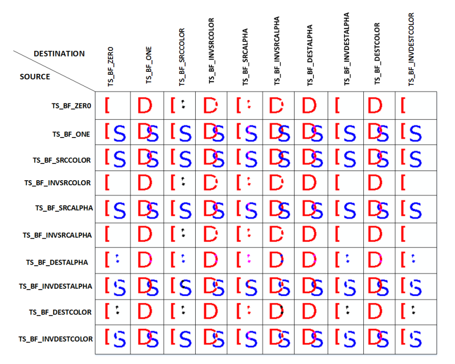
The Color and Alpha values range from 0 to 1, therefore each calculation result is also clamped to the same range. The available Blend Factors and the resulting RGBA values are listed in the table below. The effect of the blending modes is shown in the figure below.
| Blending Mode Name | Blend Factors (Sc or Df ) | RGBA Value | Definition |
|---|---|---|---|
| DSBF_ZERO |
0 |
0,0,0,0 |
|
| DSBF_ONE |
1 |
1,1,1,1 |
|
| DSBF_SRCCOLOR |
Sc |
Rsrc, Gsrc, Bsrc, Asrc |
|
| DSBF_INVSRCCOLOR |
(1 – Sc) |
1 – Rsrc, 1 – Gsrc, 1–Bsrc, 1 – Asrc |
|
| DSBF_SRCALPHA |
Sa |
Asrc, Asrc, Asrc, Asrc |
|
| DSBF_INVSRCALPHA |
(1 – Sa) |
1 – Asrc, 1 – Asrc, 1 – Asrc, 1 – Asrc |
|
| DSBF_DESTALPHA |
Da |
Adst, Adst, Adst, Adst |
|
| DSBF_INVDESTALPHA |
(1 – Da) |
1 – Adst, 1 – Adst, 1 – Adst, 1 – Adst |
|
| DSBF_DESTCOLOR |
Dc |
Rdst, Gdst, Bdst, Adst |
|
| DSBF_INVDESTCOLOR |
(1 – Dc) |
1 – Rdst, 1 – Gdst, 1 – Bdst, 1 – Adst | |
| DSBF_CONSTCOLOR |
Cc |
Rconst, Gconst, Bconst, Aconst |
|
| DSBF_CONSTALPHA |
Ca |
Aconst, Aconst, Aconst, Aconst |
|
| DSBF_UNKNOWN |
0 |
0,0,0,0 |
Framebuffer Compression
Framebuffer compression operates in screen blocks (4 x 4 pixel blocks) and achieves TSCTM4, TSCTM6 and TSCTM6a lossy, fixed-ratio compression depending on the configuration.
- TSCTM4 is a 6:1 compression (4bpp).
- TSCTM6 is a 4:1 compression (6bpp).
- TSCTM6a is a 4:1 compression (6bpp) with alpha channel.
Compression is performed at run time using minimal hardware. Pixel data can be stored in the framebuffer in compressed form and decompressed in the display control (DC) module. The output of the TSCTM4 compression is 64 bits per 4 x 4 block of pixels, and the output of the TSCTM6 compression is 96 bits per 4 x 4 block of pixels.
Color Modes
The GPU supports multiple color formats. The supported color formats are the following:
- RGBX8888 32-bit
| Pixel 0 | |||||||||||||||||||||||||||||||
|---|---|---|---|---|---|---|---|---|---|---|---|---|---|---|---|---|---|---|---|---|---|---|---|---|---|---|---|---|---|---|---|
31 |
30 |
29 |
28 |
27 |
26 |
25 |
24 |
23 |
22 |
21 |
20 |
19 |
18 |
17 |
16 |
15 |
14 |
13 |
12 |
11 |
10 |
9 |
8 |
7 |
6 |
5 |
4 |
3 |
2 |
1 |
0 |
X7 |
X6 |
X5 |
X4 |
X3 |
X2 |
X1 |
X0 |
B7 |
B6 |
B5 |
B4 |
B3 |
B2 |
B1 |
B0 |
G7 |
G6 |
G5 |
G4 |
G3 |
G2 |
G1 |
G1 |
R7 |
R6 |
R5 |
R4 |
R3 |
R2 |
R1 |
R0 |
Byte 3 |
Byte 2 |
Byte 1 |
Byte 0 |
||||||||||||||||||||||||||||
- RGBA8888 32-bit
| Pixel 0 | |||||||||||||||||||||||||||||||
|---|---|---|---|---|---|---|---|---|---|---|---|---|---|---|---|---|---|---|---|---|---|---|---|---|---|---|---|---|---|---|---|
31 |
30 |
29 |
28 |
27 |
26 |
25 |
24 |
23 |
22 |
21 |
20 |
19 |
18 |
17 |
16 |
15 |
14 |
13 |
12 |
11 |
10 |
9 |
8 |
7 |
6 |
5 |
4 |
3 |
2 |
1 |
0 |
A7 |
A6 |
A5 |
A4 |
A3 |
A2 |
A1 |
A0 |
B7 |
B6 |
B5 |
B4 |
B3 |
B2 |
B1 |
B0 |
G7 |
G6 |
G5 |
G4 |
G3 |
G2 |
G1 |
G1 |
R7 |
R6 |
R5 |
R4 |
R3 |
R2 |
R1 |
R0 |
Byte 3 |
Byte 2 |
Byte 1 |
Byte 0 |
||||||||||||||||||||||||||||
- XRGB8888 32-bit
| Pixel 0 | |||||||||||||||||||||||||||||||
|---|---|---|---|---|---|---|---|---|---|---|---|---|---|---|---|---|---|---|---|---|---|---|---|---|---|---|---|---|---|---|---|
31 |
30 |
29 |
28 |
27 |
26 |
25 |
24 |
23 |
22 |
21 |
20 |
19 |
18 |
17 |
16 |
15 |
14 |
13 |
12 |
11 |
10 |
9 |
8 |
7 |
6 |
5 |
4 |
3 |
2 |
1 |
0 |
B7 |
B6 |
B5 |
B4 |
B3 |
B2 |
B1 |
B0 |
G7 |
G6 |
G5 |
G4 |
G3 |
G2 |
G1 |
G1 |
R7 |
R6 |
R5 |
R4 |
R3 |
R2 |
R1 |
R0 |
X7 |
X6 |
X5 |
X4 |
X3 |
X2 |
X1 |
X0 |
Byte 3 |
Byte 2 |
Byte 1 |
Byte 0 |
||||||||||||||||||||||||||||
- ARGB8888 32-bit
| Pixel 0 | |||||||||||||||||||||||||||||||
|---|---|---|---|---|---|---|---|---|---|---|---|---|---|---|---|---|---|---|---|---|---|---|---|---|---|---|---|---|---|---|---|
31 |
30 |
29 |
28 |
27 |
26 |
25 |
24 |
23 |
22 |
21 |
20 |
19 |
18 |
17 |
16 |
15 |
14 |
13 |
12 |
11 |
10 |
9 |
8 |
7 |
6 |
5 |
4 |
3 |
2 |
1 |
0 |
B7 |
B6 |
B5 |
B4 |
B3 |
B2 |
B1 |
B0 |
G7 |
G6 |
G5 |
G4 |
G3 |
G2 |
G1 |
G1 |
R7 |
R6 |
R5 |
R4 |
R3 |
R2 |
R1 |
R0 |
A7 |
A6 |
A5 |
A4 |
A3 |
A2 |
A1 |
A0 |
Byte 3 |
Byte 2 |
Byte 1 |
Byte 0 |
||||||||||||||||||||||||||||
- RGB5650 16-bit
| Pixel 0 | |||||||||||||||
|---|---|---|---|---|---|---|---|---|---|---|---|---|---|---|---|
15 |
14 |
13 |
12 |
11 |
10 |
9 |
8 |
7 |
6 |
5 |
4 |
3 |
2 |
1 |
0 |
R4 |
R3 |
R2 |
R1 |
R0 |
G5 |
G4 |
G3 |
G2 |
G1 |
G1 |
B4 |
B3 |
B2 |
B1 |
B0 |
Byte 1 |
Byte 0 |
||||||||||||||
- RGBA5551 16-bit
| Pixel 0 | |||||||||||||||
|---|---|---|---|---|---|---|---|---|---|---|---|---|---|---|---|
15 |
14 |
13 |
12 |
11 |
10 |
9 |
8 |
7 |
6 |
5 |
4 |
3 |
2 |
1 |
0 |
R4 |
R3 |
R2 |
R1 |
R0 |
G4 |
G3 |
G2 |
G1 |
G1 |
B4 |
B3 |
B2 |
B1 |
B0 |
A0 |
Byte 1 |
Byte 0 |
||||||||||||||
- RGBA4444 16-bit
| Pixel 0 | |||||||||||||||
|---|---|---|---|---|---|---|---|---|---|---|---|---|---|---|---|
15 |
14 |
13 |
12 |
11 |
10 |
9 |
8 |
7 |
6 |
5 |
4 |
3 |
2 |
1 |
0 |
R3 |
R2 |
R1 |
R0 |
G3 |
G2 |
G1 |
G1 |
B3 |
B2 |
B1 |
B0 |
A3 |
A2 |
A1 |
A0 |
Byte 1 |
Byte 0 |
||||||||||||||
- RGBA0008 8-bit
| Pixel 0 | |||||||
|---|---|---|---|---|---|---|---|
7 |
6 |
5 |
4 |
3 |
2 |
1 |
0 |
A7 |
A6 |
A5 |
A4 |
A3 |
A2 |
A1 |
A0 |
Byte 0 |
|||||||
- L8 8-bit
| Pixel 0 | |||||||
|---|---|---|---|---|---|---|---|
7 |
6 |
5 |
4 |
3 |
2 |
1 |
0 |
L7 |
L6 |
L5 |
L4 |
L3 |
L2 |
L1 |
L0 |
Byte 0 |
|||||||
- L1 big-endian 1-bit
| Pixel 0 | Pixel 1 | Pixel 2 | Pixel 3 | Pixel 4 | Pixel 5 | Pixel 6 | Pixel 7 |
|---|---|---|---|---|---|---|---|
7 |
6 |
5 |
4 |
3 |
2 |
1 |
0 |
L0 |
L0 |
L0 |
L0 |
L0 |
L0 |
L0 |
L0 |
Byte 0 |
|||||||
- A1 big-endian 1-bit
| Pixel 0 | Pixel 1 | Pixel 2 | Pixel 3 | Pixel 4 | Pixel 5 | Pixel 6 | Pixel 7 |
|---|---|---|---|---|---|---|---|
7 |
6 |
5 |
4 |
3 |
2 |
1 |
0 |
A0 |
A0 |
A0 |
A0 |
A0 |
A0 |
A0 |
A0 |
Byte 0 |
|||||||
- UYVY 32-bit 2-pixel
| Pixel 1 | Pixel1&0 | Pixel 0 | Pixel1&0 | ||||||||||||||||||||||||||||
|---|---|---|---|---|---|---|---|---|---|---|---|---|---|---|---|---|---|---|---|---|---|---|---|---|---|---|---|---|---|---|---|
31 |
30 |
29 |
28 |
27 |
26 |
25 |
24 |
23 |
22 |
21 |
20 |
19 |
18 |
17 |
16 |
15 |
14 |
13 |
12 |
11 |
10 |
9 |
8 |
7 |
6 |
5 |
4 |
3 |
2 |
1 |
0 |
Y7 |
Y6 |
Y5 |
Y4 |
Y3 |
Y2 |
Y1 |
Y0 |
V7 |
V6 |
V5 |
V4 |
V3 |
V2 |
V1 |
V0 |
Y7 |
Y6 |
Y5 |
Y4 |
Y3 |
Y2 |
Y1 |
Y1 |
U7 |
U6 |
U5 |
U4 |
U3 |
U2 |
U1 |
U0 |
Byte 3 |
Byte 2 |
Byte 1 |
Byte 0 |
||||||||||||||||||||||||||||
- ABGR8888 32-bit
| Pixel 0 | |||||||||||||||||||||||||||||||
|---|---|---|---|---|---|---|---|---|---|---|---|---|---|---|---|---|---|---|---|---|---|---|---|---|---|---|---|---|---|---|---|
31 |
30 |
29 |
28 |
27 |
26 |
25 |
24 |
23 |
22 |
21 |
20 |
19 |
18 |
17 |
16 |
15 |
14 |
13 |
12 |
11 |
10 |
9 |
8 |
7 |
6 |
5 |
4 |
3 |
2 |
1 |
0 |
R7 |
R6 |
R5 |
R4 |
R3 |
R2 |
R1 |
R0 |
G7 |
G6 |
G5 |
G4 |
G3 |
G2 |
G1 |
G1 |
B7 |
B6 |
B5 |
B4 |
B3 |
B2 |
B1 |
B0 |
A7 |
A6 |
A5 |
A4 |
A3 |
A2 |
A1 |
A0 |
Byte 3 |
Byte 2 |
Byte 1 |
Byte 0 |
||||||||||||||||||||||||||||
- BGRA 32-bit
| Pixel 0 | |||||||||||||||||||||||||||||||
|---|---|---|---|---|---|---|---|---|---|---|---|---|---|---|---|---|---|---|---|---|---|---|---|---|---|---|---|---|---|---|---|
31 |
30 |
29 |
28 |
27 |
26 |
25 |
24 |
23 |
22 |
21 |
20 |
19 |
18 |
17 |
16 |
15 |
14 |
13 |
12 |
11 |
10 |
9 |
8 |
7 |
6 |
5 |
4 |
3 |
2 |
1 |
0 |
A7 |
A6 |
A5 |
A4 |
A3 |
A2 |
A1 |
A0 |
R7 |
R6 |
R5 |
R4 |
R3 |
R2 |
R1 |
R0 |
G7 |
G6 |
G5 |
G4 |
G3 |
G2 |
G1 |
G1 |
B7 |
B6 |
B5 |
B4 |
B3 |
B2 |
B1 |
B0 |
Byte 3 |
Byte 2 |
Byte 1 |
Byte 0 |
||||||||||||||||||||||||||||
- BGRX 32-bit
| Pixel 0 | |||||||||||||||||||||||||||||||
|---|---|---|---|---|---|---|---|---|---|---|---|---|---|---|---|---|---|---|---|---|---|---|---|---|---|---|---|---|---|---|---|
31 |
30 |
29 |
28 |
27 |
26 |
25 |
24 |
23 |
22 |
21 |
20 |
19 |
18 |
17 |
16 |
15 |
14 |
13 |
12 |
11 |
10 |
9 |
8 |
7 |
6 |
5 |
4 |
3 |
2 |
1 |
0 |
X7 |
X6 |
X5 |
X4 |
X3 |
X2 |
X1 |
X0 |
R7 |
R6 |
R5 |
R4 |
R3 |
R2 |
R1 |
R0 |
G7 |
G6 |
G5 |
G4 |
G3 |
G2 |
G1 |
G1 |
B7 |
B6 |
B5 |
B4 |
B3 |
B2 |
B1 |
B0 |
Byte 3 |
Byte 2 |
Byte 1 |
Byte 0 |
||||||||||||||||||||||||||||
- TSC4 16-pixel/64-bit
- TSC6 16-pixel/96-bit
- TSC6A 16-pixel with Alpha/96-bit
- A1LE little-endian 1-bit
| Pixel 7 | Pixel 6 | Pixel 5 | Pixel 4 | Pixel 3 | Pixel 2 | Pixel 1 | Pixel 0 |
|---|---|---|---|---|---|---|---|
7 |
6 |
5 |
4 |
3 |
2 |
1 |
0 |
A0 |
A0 |
A0 |
A0 |
A0 |
A0 |
A0 |
A0 |
Byte 0 |
|||||||
- A2LE little-endian 2-bit
| Pixel 3 | Pixel 2 | Pixel 1 | Pixel 0 | ||||
|---|---|---|---|---|---|---|---|
7 |
6 |
5 |
4 |
3 |
2 |
1 |
0 |
A1 |
A0 |
A1 |
A0 |
A1 |
A0 |
A1 |
A0 |
Byte 0 |
|||||||
- A4LE little-endian 4-bit
| Pixel 1 | Pixel 0 | ||||||
|---|---|---|---|---|---|---|---|
7 |
6 |
5 |
4 |
3 |
2 |
1 |
0 |
A3 |
A2 |
A1 |
A0 |
A3 |
A2 |
A1 |
A0 |
Byte 0 |
|||||||
- L1LE little-endian 1-bit
| Pixel 7 | Pixel 6 | Pixel 5 | Pixel 4 | Pixel 3 | Pixel 2 | Pixel 1 | Pixel 0 |
|---|---|---|---|---|---|---|---|
7 |
6 |
5 |
4 |
3 |
2 |
1 |
0 |
L0 |
L0 |
L0 |
L0 |
L0 |
L0 |
L0 |
L0 |
Byte 0 |
|||||||
- L2LE little-endian 2-bit
| Pixel 3 | Pixel 2 | Pixel 1 | Pixel 0 | ||||
|---|---|---|---|---|---|---|---|
7 |
6 |
5 |
4 |
3 |
2 |
1 |
0 |
L1 |
L0 |
L1 |
L0 |
L1 |
L0 |
L1 |
L0 |
Byte 0 |
|||||||
- L4LE little-endian 4-bit
| Pixel 1 | Pixel 0 | ||||||
|---|---|---|---|---|---|---|---|
7 |
6 |
5 |
4 |
3 |
2 |
1 |
0 |
L3 |
L2 |
L1 |
L0 |
L3 |
L2 |
L1 |
L0 |
Byte 0 |
|||||||
- A2 big-endian 2-bit
| Pixel 0 | Pixel 1 | Pixel 2 | Pixel 3 | ||||
|---|---|---|---|---|---|---|---|
7 |
6 |
5 |
4 |
3 |
2 |
1 |
0 |
A1 |
A0 |
A1 |
A0 |
A1 |
A0 |
A1 |
A0 |
Byte 0 |
|||||||
- L2 big-endian 2-bit
| Pixel 0 | Pixel 1 | Pixel 2 | Pixel 3 | ||||
|---|---|---|---|---|---|---|---|
7 |
6 |
5 |
4 |
3 |
2 |
1 |
0 |
L1 |
L0 |
L1 |
L0 |
L1 |
L0 |
L1 |
L0 |
Byte 0 |
|||||||
- A4 big-endian 4-bit
| Pixel 0 | Pixel 1 | ||||||
|---|---|---|---|---|---|---|---|
7 |
6 |
5 |
4 |
3 |
2 |
1 |
0 |
A3 |
A2 |
A1 |
A0 |
A3 |
A2 |
A1 |
A0 |
Byte 0 |
|||||||
- L4 big-endian 4-bit
| Pixel 0 | Pixel 1 | ||||||
|---|---|---|---|---|---|---|---|
7 |
6 |
5 |
4 |
3 |
2 |
1 |
0 |
L3 |
L2 |
L1 |
L0 |
L3 |
L2 |
L1 |
L0 |
Byte 0 |
|||||||
- RGBA3320 8-bit
| Pixel 0 | |||||||
|---|---|---|---|---|---|---|---|
7 |
6 |
5 |
4 |
3 |
2 |
1 |
0 |
R2 |
R1 |
R0 |
G2 |
G1 |
G0 |
B1 |
B0 |
Byte 0 |
|||||||
- BGR24 24-bit
| Pixel 0 | |||||||||||||||||||||||
|---|---|---|---|---|---|---|---|---|---|---|---|---|---|---|---|---|---|---|---|---|---|---|---|
23 |
22 |
21 |
20 |
19 |
18 |
17 |
16 |
15 |
14 |
13 |
12 |
11 |
10 |
9 |
8 |
7 |
6 |
5 |
4 |
3 |
2 |
1 |
0 |
R7 |
R6 |
R5 |
R4 |
R3 |
R2 |
R1 |
R0 |
G7 |
G6 |
G5 |
G4 |
G3 |
G2 |
G1 |
G0 |
B7 |
B6 |
B5 |
B4 |
B3 |
B2 |
B1 |
B0 |
Byte 2 |
Byte 1 |
Byte 0 |
|||||||||||||||||||||
- RGB24 24-bit
| Pixel 0 | |||||||||||||||||||||||
|---|---|---|---|---|---|---|---|---|---|---|---|---|---|---|---|---|---|---|---|---|---|---|---|
23 |
22 |
21 |
20 |
19 |
18 |
17 |
16 |
15 |
14 |
13 |
12 |
11 |
10 |
9 |
8 |
7 |
6 |
5 |
4 |
3 |
2 |
1 |
0 |
B7 |
B6 |
B5 |
B4 |
B3 |
B2 |
B1 |
B0 |
G7 |
G6 |
G5 |
G4 |
G3 |
G2 |
G1 |
G0 |
R7 |
R6 |
R5 |
R4 |
R3 |
R2 |
R1 |
R0 |
Byte 2 |
Byte 1 |
Byte 0 |
|||||||||||||||||||||
Color Expansion
The internal format is always on RGBA8888 32-bit format. Therefore, lower-order color formats are expanded to 8 bits per color channel. This is achieved by high-order bit replication. For example, a 5-bit color format is constructed as follows:
Instruction Set Architecture
The microarchitecture of the GPU for fragment processing is a four-issue VLIW core. Each VLIW instruction is 64 bits’ long and consists of four sub-instructions (corresponding to sub-operations). The sub-operations for the GPU are: i) instructions for Alpha channel arithmetic operations (SUBOP0); ii) instructions for RGB vector arithmetic operations (SUBOP1); iii) memory addressing instructions for reading and writing to memory (SUBOP2); and iv) branching instructions based on comparisons between RGB or Alpha values (SUBOP3).
Each VLIW bundle is designed to perform six arithmetic operations per cycle (simultaneously). If more than one VLIW bundle is enabled, the addressing sub-operations (SUBOP2) are issued once for all the enabled bundles while the remaining sub-operations (SUBOP0, SUBOP1, and SUBOP3) are issued once for each VLIW bundle.
Registers
TEX0_BASE
- Name: Base Address Register 0
- Description: This register specifies the base address of drawing surface 0.
- Base Address: 0x40028000
- Offset: 0x0
- Reset Value: 0x00000000
| Bits | Field Name | RW | Reset | Description |
|---|---|---|---|---|
31:0 |
RW |
0x0 |
Specifies the base address of drawing surface 0. |
TEX0_FSTRIDE
- Name: Image Stride Register 0
- Description: This register specifies image 0 mode and stride.
- Base Address: 0x40028000
- Offset: 0x4
- Reset Value: 0x00000000
| Bits | Field Name | RW | Reset | Description |
|---|---|---|---|---|
31 |
RW |
0x0 |
If set for destination texture, color dithering is enabled. (Applicable to output formats: RGBA5650, RGBA5551, and RGBA4444). |
|
30:24 |
RW |
0x0 |
Specifies the image format.
|
|
23:16 |
RW |
0x0 |
Specifies the image mode.
|
|
15:0 |
RW |
0x0 |
Specifies the image stride distance in bytes from one scanline to another (signed). |
TEX0_RESXY
- Name: Image Size Register 0
- Description: This register specifies the size of image 0 resolution.
- Base Address: 0x40028000
- Offset: 0x8
- Reset Value: 0x00000000
| Bits | Field Name | RW | Reset | Description |
|---|---|---|---|---|
31:16 |
RW |
0x0 |
Specifies the size of resolution Y. |
|
15:0 |
RW |
0x0 |
Specifies the size of resolution X. |
TEX1_BASE
- Name: Base Address Register 1
- Description: This register specifies the base address of drawing surface 1.
- Base Address: 0x40028000
- Offset: 0x10
- Reset Value: 0x00000000
| Bits | Field Name | RW | Reset | Description |
|---|---|---|---|---|
31:0 |
RW |
0x0 |
Specifies the base address of drawing surface 1. |
TEX1_FSTRIDE
- Name: Image Stride Register 1
- Description: This register specifies image 1 mode and stride.
- Base Address: 0x40028000
- Offset: 0x14
- Reset Value: 0x00000000
| Bits | Field Name | RW | Reset | Description |
|---|---|---|---|---|
31 |
RW |
0x0 |
If set for destination texture, enables color dithering. (Applicable to output formats: RGBA5650, RGBA5551, and RGBA4444). |
|
30:24 |
RW |
0x0 |
Specifies the image format.
|
|
23:16 |
RW |
0x0 |
Specifies the image mode.
|
|
15:0 |
RW |
0x0 |
Specifies the image stride distance in bytes from one scanline to another (signed). |
TEX1_RESXY
- Name: Image Size Register 1
- Description: This register specifies the size of image 1 resolution.
- Base Address: 0x40028000
- Offset: 0x18
- Reset Value: 0x00000000
| Bits | Field Name | RW | Reset | Description |
|---|---|---|---|---|
31:16 |
RW |
0x0 |
Specifies the size of resolution Y. |
|
15:0 |
RW |
0x0 |
Specifies the size of resolution X. |
TEX_COLOR
- Name: Color Register
- Description: This register specifies texture map’s default color.
- Base Address: 0x40028000
- Offset: 0x1C
- Reset Value: 0x00000000
| Bits | Field Name | RW | Reset | Description |
|---|---|---|---|---|
31:24 |
RW |
0x0 |
Specifies the Alpha (A) value. |
|
23:16 |
RW |
0x0 |
Specifies the Blue (B) value. |
|
15:8 |
RW |
0x0 |
Specifies the Green (G) value. |
|
7:0 |
RW |
0x0 |
Specifies the Red (R) value. |
TEX2_BASE
- Name: Base Address Register 2
- Description: This register specifies the base address of drawing surface 2.
- Base Address: 0x40028000
- Offset: 0x20
- Reset Value: 0x00000000
| Bits | Field Name | RW | Reset | Description |
|---|---|---|---|---|
31:0 |
RW |
0x0 |
Specifies the base address of drawing surface 2. |
TEX2_FSTRIDE
- Name: Image Stride Register 2
- Description: This register specifies image 2 mode and stride.
- Base Address: 0x40028000
- Offset: 0x24
- Reset Value: 0x00000000
| Bits | Field Name | RW | Reset | Description |
|---|---|---|---|---|
31 |
RW |
0x0 |
If set for destination texture, color dithering is enabled. (Applicable to output formats: RGBA5650, RGBA5551, and RGBA4444). |
|
30:24 |
RW |
0x0 |
Specifies the image format.
|
|
23:16 |
RW |
0x0 |
Specifies the image mode.
|
|
15:0 |
RW |
0x0 |
Specifies the image stride distance in bytes from one scanline to another (signed). |
TEX2_RESXY
- Name: Image Size Register 2
- Description: This register specifies the size of image 2 resolution.
- Base Address: 0x40028000
- Offset: 0x28
- Reset Value: 0x00000000
| Bits | Field Name | RW | Reset | Description |
|---|---|---|---|---|
31:16 |
RW |
0x0 |
Specifies the size of resolution Y. |
|
15:0 |
RW |
0x0 |
Specifies the size of resolution X. |
TEX3_BASE
- Name: Base Address Register 3
- Description: This register specifies the base address of drawing surface 3.
- Base Address: 0x40028000
- Offset: 0x30
- Reset Value: 0x00000000
| Bits | Field Name | RW | Reset | Description |
|---|---|---|---|---|
31:0 |
RW |
0x0 |
Specifies the base address of drawing surface 3. |
TEX3_FSTRIDE
- Name: Image Stride Register 3
- Description: This register specifies image 3 mode and stride.
- Base Address: 0x40028000
- Offset: 0x34
- Reset Value: 0x00000000
| Bits | Field Name | RW | Reset | Description |
|---|---|---|---|---|
31 |
RW |
0x0 |
If set for destination texture, color dithering is enabled. (Applicable to output formats: RGBA5650, RGBA5551, and RGBA4444). |
|
30:24 |
RW |
0x0 |
Specifies the image format.
|
|
23:16 |
RW |
0x0 |
Specifies the image mode.
|
|
15:0 |
RW |
0x0 |
Specifies the image stride distance in bytes from one scanline to another (signed). |
TEX3_RESXY
- Name: Image Size Register 3
- Description: This register specifies the size of image 3 resolution.
- Base Address: 0x40028000
- Offset: 0x38
- Reset Value: 0x00000000
| Bits | Field Name | RW | Reset | Description |
|---|---|---|---|---|
31:16 |
RW |
0x0 |
Specifies the size of resolution Y. |
|
15:0 |
RW |
0x0 |
Specifies the size of resolution X. |
BREAKPOINT
- Name: Break Point Register
- Description: This register specifies the break point.
- Base Address: 0x40028000
- Offset: 0x80
- Reset Value: 0x00000000
| Bits | Field Name | RW | Reset | Description |
|---|---|---|---|---|
31:0 |
RW |
0x0 |
BREAKPOINT_MASK
- Name: Break Point Mask Register
- Description: This register specifies the break point mask.
- Base Address: 0x40028000
- Offset: 0x8C
- Reset Value: 0x00000000
| Bits | Field Name | RW | Reset | Description |
|---|---|---|---|---|
31:0 |
RW |
0x0 |
CG_CTRL
- Name: Clock Gating Control Register
- Description: This register controls the clock gating.
- Base Address: 0x40028000
- Offset: 0x94
- Reset Value: 0x00000000
| Bits | Field Name | RW | Reset | Description |
|---|---|---|---|---|
31 |
RW |
0x0 |
Disable clock gating for all modules. |
|
30:28 |
RSVD |
R |
Reserved bits |
|
27 |
RW |
0x0 |
Disable clock gating for Core 0 Instruction Memory. |
|
26:24 |
RSVD |
R |
Reserved bits |
|
23 |
RW |
0x0 |
Disable clock gating for Core 0. |
|
22:20 |
RSVD |
R |
Reserved bits |
|
19 |
RW |
0x0 |
Disable clock gating for Core 0 Scheduler. |
|
18:16 |
RSVD |
R |
Reserved bits |
|
15 |
RW |
0x0 |
Disable clock gating for Core 0 Register File. |
|
14:12 |
RSVD |
R |
Reserved bits |
|
11 |
RW |
0x0 |
Disable clock gating for Core 0 Pipeline. |
|
10:8 |
RSVD |
R |
Reserved bits |
|
7 |
RW |
0x0 |
Disable clock gating for the BusInterface (memory system). |
|
6:4 |
RSVD |
R |
Reserved bits |
|
3 |
RW |
0x0 |
Disable clock gating for the Render Output Unit of Core 0. |
|
2 |
RSVD |
R |
Reserved bit |
|
1 |
RW |
0x0 |
Disable clock gating for the NemaP Configuration Register File. |
|
0 |
RW |
0x0 |
Disable clock gating for the Command List Processor. |
DIRTYMIN
- Name: Dirty Region Min Register
- Description: This register reads the Dirty_Min value and resets dirty region to resolution size on write function.
- Base Address: 0x40028000
- Offset: 0x98
- Reset Value: 0xFFFFFFFF
| Bits | Field Name | RW | Reset | Description |
|---|---|---|---|---|
31:0 |
RW |
0xFFFFFFFF |
Write any value to reset dirty region to resolution size. Read the Dirty_Min value. |
DIRTYMAX
- Name: Dirty Region Max Register
- Description: This register reads the Dirty_Max value.
- Base Address: 0x40028000
- Offset: 0x9C
- Reset Value: 0x00000000
| Bits | Field Name | RW | Reset | Description |
|---|---|---|---|---|
31:0 |
R |
0x0 |
Read the Dirty_Max value. |
IMEM_ADDR
- Name: Load Shader Instruction Memory Address Register
- Description: This register specifies the load shader instruction memory address.
- Base Address: 0x40028000
- Offset: 0xC4
- Reset Value: 0x00000000
| Bits | Field Name | RW | Reset | Description |
|---|---|---|---|---|
31:4 |
RSVD |
R |
Reserved bits |
|
3:0 |
RW |
0x0 |
Specifies the load shader instruction memory address. |
IMEM_DATA_LOW
- Name: Lower Bit Data Register
- Description: This register specifies the lower bits (31: 0) of the 64-bit load shader instruction memory data.
- Base Address: 0x40028000
- Offset: 0xC8
- Reset Value: 0x00000000
| Bits | Field Name | RW | Reset | Description |
|---|---|---|---|---|
31:0 |
RW |
0x0 |
Specifies the lower bits (31:0) of the load shader instruction memory data. |
IMEM_DATA_HIGH
- Name: Higher Bit Data Register
- Description: This register specifies the higher bits (63-32) of the 64-bit load shader instruction memory data.
- Base Address: 0x40028000
- Offset: 0xCC
- Reset Value: 0x00000000
| Bits | Field Name | RW | Reset | Description |
|---|---|---|---|---|
31:0 |
RW |
0x0 |
Specifies the higher bits (63-32) of the load shader instruction memory data. |
FLUSH_CTRL
- Name: System Flush Register
- Description: This register controls the system flush.
- Base Address: 0x40028000
- Offset: 0xE4
- Reset Value: 0x00000007
| Bits | Field Name | RW | Reset | Description |
|---|---|---|---|---|
31:14 |
RSVD |
R |
Reserved bits |
|
13 |
RW |
0x0 |
When set to 1, the write caches are flushed. |
|
12 |
RSVD |
R |
Reserved bit |
|
11 |
RW |
0x0 |
If set to 1, the write caches are flushed when the host triggers the rasterizer register (NEMA_DRAW_CMD_NOHOLD). |
|
10:8 |
RSVD |
R |
Reserved bits |
|
7 |
RW |
0x0 |
If set to 1, the write caches are flushed when the Command List Processor triggers the rasterizer register (NEMA_DRAW_CMD_NOHOLD). |
|
6 |
RW |
0x0 |
When set to 1, the read caches are flushed. |
|
5 |
RSVD |
R |
Reserved bit |
|
4 |
RW |
0x0 |
If set to 1, the read caches are flushed when the host triggers the rasterizer register (NEMA_DRAW_CMD_NOHOLD) |
|
3:1 |
RSVD |
R |
Reserved bits |
|
0 |
RW |
0x1 |
If set to 1, the read caches are flushed when the Command List Processor triggers the rasterizer register (NEMA_DRAW_CMD_NOHOLD). |
CMD_STAT
- Name: Command Status Register
- Description: This register shows the command status.
- Base Address: 0x40028000
- Offset: 0xE8
- Reset Value: 0x00000000
| Bits | Field Name | RW | Reset | Description |
|---|---|---|---|---|
31 |
RW |
0x0 |
Indicates if the Command List Processor is busy. |
|
30 |
RW |
0x0 |
Indicates if there are data available in System Memory. |
|
29 |
RW |
0x0 |
Indicates if there are available data to read from FIFO. |
|
28 |
RW |
0x0 |
Shows many cells are still available in FIFO. |
|
27:18 |
RSVD |
R |
Reserved bits |
|
17:13 |
RW |
0x0 |
Shows many cells are still available in FIFO. |
|
12 |
RSVD |
R |
Reserved bit |
|
11:9 |
RW |
0x0 |
Shows the address of the stack pointer. |
|
8:7 |
RSVD |
R |
Reserved bits |
|
6:4 |
RW |
0x0 |
Indicates the state of CMDList internal FSM. |
|
3:1 |
RSVD |
R |
Reserved bits |
|
0 |
RW |
0x0 |
Indicates the state of the FSM responsible for fetching. |
RING_BUF_STORE
- Name: Ring Buffer Register
- Description: This register stores the Ring Buffer’s last written address.
- Base Address: 0x40028000
- Offset: 0xEC
- Reset Value: 0x00000000
| Bits | Field Name | RW | Reset | Description |
|---|---|---|---|---|
31:0 |
RW |
0x0 |
Stores the last written address of the ring buffer. |
CMD_ADDR
- Name: Command List Base Address Register
- Description: This register specifies the command list base address.
- Base Address: 0x40028000
- Offset: 0xF0
- Reset Value: 0x00000000
| Bits | Field Name | RW | Reset | Description |
|---|---|---|---|---|
31:0 |
RW |
0x0 |
Specifies the base address of every new command list ready to be executed. |
CMD_SIZE
- Name: Command List Size Register
- Description: This register specifies the command list size.
- Base Address: 0x40028000
- Offset: 0xF4
- Reset Value: 0x00000000
| Bits | Field Name | RW | Reset | Description |
|---|---|---|---|---|
31:0 |
RW |
0x0 |
Specifies the length of the command list ready to be executed. |
INT_CTRL
- Name: Interrupt Control Register
- Description: This register controls the interrupt.
- Base Address: 0x40028000
- Offset: 0xF8
- Reset Value: 0x00000000
| Bits | Field Name | RW | Reset | Description |
|---|---|---|---|---|
31:30 |
RW |
0x0 |
Specifies the core_clk_dvfs output. |
|
29:28 |
RSVD |
R |
Reserved bits |
|
27 |
RW |
0x0 |
When set to 1, the throttle signal will be ignored. |
|
26:4 |
RSVD |
R |
Reserved bits |
|
3 |
RW |
0x0 |
When set to 1, the interrupt in the NEMA_IRQ_ID register is cleared. |
|
2 |
RW |
0x0 |
When set to 1, an interrupt is signaled at the end of a drawing command. |
|
1 |
RW |
0x0 |
When set to 1, an interrupt is signaled at the end of a command list. |
|
0 |
RW |
0x0 |
|
STAT
- Name: GPU Status Register
- Description: This register shows the GPU status.
- Base Address: 0x40028000
- Offset: 0xFC
- Reset Value: 0x00000000
| Bits | Field Name | RW | Reset | Description |
|---|---|---|---|---|
31 |
RW |
0x0 |
Indicates if the system is busy. |
|
30 |
RW |
0x0 |
Indicates if the bus interface unit is busy. |
|
29 |
RW |
0x0 |
Indicates if the command list bus is busy. |
|
28 |
RW |
0x0 |
Indicates if the Command List Processor is busy. |
|
27:24 |
RW |
0x0 |
Indicate if the rasterizer unit is busy. |
|
23:13 |
RSVD |
R |
Reserved bits |
|
12 |
RW |
0x0 |
Indicates if the Core 0 render output unit is busy. |
|
11:9 |
RSVD |
R |
Reserved bits |
|
8 |
RW |
0x0 |
Indicates if the Core 0 texture map unit is busy. |
|
7:5 |
RSVD |
R |
Reserved bits |
|
4 |
RW |
0x0 |
Indicates if the Core 0 graphics pipeline is busy. |
|
3:1 |
RSVD |
R |
Reserved bits |
|
0 |
RW |
0x0 |
Indicates if the Core 0 is busy. |
DRAW_CMD_NOHOLD
- Name: Rasterizer Command Register
- Description: This register controls the rasterizer.
- Base Address: 0x40028000
- Offset: 0x100
- Reset Value: 0x00000000
| Bits | Field Name | RW | Reset | Description |
|---|---|---|---|---|
31 |
RSVD |
R |
Reserved bit |
|
30 |
RW |
0x0 |
When set to 1, tile mode is enabled. |
|
29 |
RW |
0x0 |
When set to 1, positive culling (counter-clockwise) is enabled. |
|
28 |
RW |
0x0 |
When set to 1, negative culling (clockwise) is enabled. |
|
27 |
RW |
0x0 |
When set to 1, color gradient is enabled. |
|
26 |
RW |
0x0 |
When set to 1, antialiasing feature is enabled for edge 0. |
|
25 |
RW |
0x0 |
When set to 1, antialiasing feature is enabled for edge 1. |
|
24 |
RW |
0x0 |
When set to 1, antialiasing feature is enabled for edge 2. |
|
23 |
RW |
0x0 |
When set to 1, antialiasing feature is enabled for edge 3. |
|
22:3 |
RSVD |
R |
Reserved bits |
|
2:0 |
RW |
0x0 |
Draw commands:
|
DRAW_STARTXY
- Name: Draw Start XY Register
- Description: This register specifies the start XY of drawing.
- Base Address: 0x40028000
- Offset: 0x104
- Reset Value: 0x00000000
| Bits | Field Name | RW | Reset | Description |
|---|---|---|---|---|
31:16 |
RW |
0x0 |
Specifies the Y coordinate (integer value) of vertex 0. |
|
15:0 |
RW |
0x0 |
Specifies the X coordinate (integer value) of vertex 0. |
DRAW_ENDXY
- Name: Draw End XY Register
- Description: This register specifies the end XY of drawing.
- Base Address: 0x40028000
- Offset: 0x108
- Reset Value: 0x00000000
| Bits | Field Name | RW | Reset | Description |
|---|---|---|---|---|
31:16 |
RW |
0x0 |
Specifies the Y coordinate (integer value) of vertex 1. |
|
15:0 |
RW |
0x0 |
Specifies the X coordinate (integer value) of vertex 1. |
CLIPMIN
- Name: Clip Min Register
- Description: This register specifies clipping rectangle upper left vertex.
- Base Address: 0x40028000
- Offset: 0x110
- Reset Value: 0x00000000
| Bits | Field Name | RW | Reset | Description |
|---|---|---|---|---|
31:16 |
RW |
0x0 |
Defines the upper left Y coordinate. |
|
15:0 |
RW |
0x0 |
Defines the upper left X coordinate. |
CLIPMAX
- Name: Clip Max Register
- Description: This register specifies clipping rectangle bottom right vertex.
- Base Address: 0x40028000
- Offset: 0x114
- Reset Value: 0x00000000
| Bits | Field Name | RW | Reset | Description |
|---|---|---|---|---|
31:16 |
RW |
0x0 |
Defines the bottom right Y coordinate. |
|
15:0 |
RW |
0x0 |
Defines the bottom right X coordinate. |
MAT_MCL
- Name: Matrix Multiplication Control Register
- Description: This register controls the rasterizer matrix multiplication.
- Base Address: 0x40028000
- Offset: 0x118
- Reset Value: 0x00000000
| Bits | Field Name | RW | Reset | Description |
|---|---|---|---|---|
31:30 |
RSVD |
R |
Reserved bits |
|
29 |
RW |
0x0 |
When set to 1, the 0.5 value is added to the X and Y coordinates. |
|
28 |
RW |
0x0 |
When set to 1, the matrix multiplications are bypassed. |
|
27 |
RW |
0x0 |
When set to 0, the result is in fixed point value (default). |
|
26 |
RW |
0x0 |
When set to 1, the result is in floating point value. |
|
25:0 |
RSVD |
R |
Reserved bits |
CODEPTR
- Name: Shader Code Register
- Description: This register specifies the pointer of the shader code.
- Base Address: 0x40028000
- Offset: 0x11C
- Reset Value: 0x00000000
| Bits | Field Name | RW | Reset | Description |
|---|---|---|---|---|
31:16 |
RW |
0x0 |
Specifies the pointer for the instruction that will be executed for the background pixels. |
|
15:0 |
RW |
0x0 |
Specifies the pointer for the instruction that will be executed for the foreground pixels. |
DRAW_PT0_X
- Name: Vertex 0 Draw X Register
- Description: This register specifies the X coordinate of vertex 0 drawing primitive.
- Base Address: 0x40028000
- Offset: 0x120
- Reset Value: 0x00000000
| Bits | Field Name | RW | Reset | Description |
|---|---|---|---|---|
31:0 |
RW |
0x0 |
Specifies the X coordinate of vertex 0 drawing primitive (16.16 fixed point). |
DRAW_PT0_Y
- Name: Vertex 0 Draw Y Register
- Description: This register specifies the Y coordinate of vertex 0 drawing primitive.
- Base Address: 0x40028000
- Offset: 0x124
- Reset Value: 0x00000000
| Bits | Field Name | RW | Reset | Description |
|---|---|---|---|---|
31:0 |
RW |
0x0 |
Specifies the Y coordinate of vertex 0 drawing primitive (16.16 fixed point). |
DRAW_COLOR
- Name: Drawing Color Register
- Description: This register specifies the drawing color for filling primitives.
- Base Address: 0x40028000
- Offset: 0x12C
- Reset Value: 0x00000000
| Bits | Field Name | RW | Reset | Description |
|---|---|---|---|---|
31:0 |
RW |
0x0 |
Specifies the drawing color for filling primitives. |
DRAW_PT1_X
- Name: Vertex 1 Draw X Register
- Description: This register specifies the X coordinate of vertex 1 drawing primitive.
- Base Address: 0x40028000
- Offset: 0x130
- Reset Value: 0x00000000
| Bits | Field Name | RW | Reset | Description |
|---|---|---|---|---|
31:0 |
RW |
0x0 |
Specifies the X coordinate of vertex 1 drawing primitive (16.16 fixed point). |
DRAW_PT1_Y
- Name: Vertex 1 Draw Y Register
- Description: This register specifies the Y coordinate of vertex 1 drawing primitive.
- Base Address: 0x40028000
- Offset: 0x134
- Reset Value: 0x00000000
| Bits | Field Name | RW | Reset | Description |
|---|---|---|---|---|
31:0 |
RW |
0x0 |
Specifies the Y coordinate of vertex 1 drawing primitive (16.16 fixed point). |
BYPASS_ADDR
- Name: Bypass Address Register
- Description: This register shows the address of bypass mode of rasterizer setup access.
- Base Address: 0x40028000
- Offset: 0x138
- Reset Value: 0x00000000
| Bits | Field Name | RW | Reset | Description |
|---|---|---|---|---|
31:0 |
RW |
0x0 |
Sets the address of bypass mode of rasterizer setup access. |
BYPASS_DATA
- Name: Bypass Data Register
- Description: This register shows the data and enablement of bypass mode of rasterizer.
- Base Address: 0x40028000
- Offset: 0x13C
- Reset Value: 0x00000000
| Bits | Field Name | RW | Reset | Description |
|---|---|---|---|---|
31:0 |
RW |
0x0 |
Shows data and enablement of bypass mode of rasterizer. |
DRAW_PT2_X
- Name: Vertex 2 Draw X Register
- Description: This register specifies the X coordinate of vertex 2 drawing primitive.
- Base Address: 0x40028000
- Offset: 0x140
- Reset Value: 0x00000000
| Bits | Field Name | RW | Reset | Description |
|---|---|---|---|---|
31:0 |
RW |
0x0 |
Specifies the X coordinate of vertex 2 drawing primitive (16.16 fixed point). |
DRAW_PT2_Y
- Name: Vertex 2 Draw Y Register
- Description: This register specifies the Y coordinate of vertex 2 drawing primitive.
- Base Address: 0x40028000
- Offset: 0x144
- Reset Value: 0x00000000
| Bits | Field Name | RW | Reset | Description |
|---|---|---|---|---|
31:0 |
RW |
0x0 |
Specifies the Y coordinate of vertex 2 drawing primitive (16.16 fixed point). |
CMD_LIST_ID
- Name: Command List ID Register
- Description: This register specifies the last executed command list.
- Base Address: 0x40028000
- Offset: 0x148
- Reset Value: 0x00000000
| Bits | Field Name | RW | Reset | Description |
|---|---|---|---|---|
31:0 |
RW |
0x0 |
Specifies the last executed command list. |
DRAW_PT3_X
- Name: Vertex 3 Draw X Register
- Description: This register specifies the X coordinate of vertex 3 drawing primitive.
- Base Address: 0x40028000
- Offset: 0x150
- Reset Value: 0x00000000
| Bits | Field Name | RW | Reset | Description |
|---|---|---|---|---|
31:0 |
RW |
0x0 |
Specifies the X coordinate of vertex 3 drawing primitive (16.16 fixed point). |
DRAW_PT3_Y
- Name: Vertex 3 Draw Y Register
- Description: This register specifies the Y coordinate of vertex 3 drawing primitive.
- Base Address: 0x40028000
- Offset: 0x154
- Reset Value: 0x00000000
| Bits | Field Name | RW | Reset | Description |
|---|---|---|---|---|
31:0 |
RW |
0x0 |
Specifies the Y coordinate of vertex 3 drawing primitive (16.16 fixed point). |
CLIPMIN1
- Name: Clip Min Register 1
- Description: This register specifies the second clipping rectangle upper left vertex.
- Base Address: 0x40028000
- Offset: 0x158
- Reset Value: 0x00000000
| Bits | Field Name | RW | Reset | Description |
|---|---|---|---|---|
31:16 |
RW |
0x0 |
Defines the upper left Y coordinate. |
|
15:0 |
RW |
0x0 |
Defines the upper left X coordinate. |
CLIPMAX1
- Name: Clip Max Register 1
- Description: This register specifies the second clipping rectangle bottom right vertex.
- Base Address: 0x40028000
- Offset: 0x15C
- Reset Value: 0x7FFF7FFF
| Bits | Field Name | RW | Reset | Description |
|---|---|---|---|---|
31:16 |
RW |
0x7FFF |
Defines the bottom right Y coordinate. |
|
15:0 |
RW |
0x7FFF |
Defines the bottom right X coordinate. |
MM00
- Name: (0,0) Matrix Register
- Description: This register specifies the (0,0) matrix floating point element.
- Base Address: 0x40028000
- Offset: 0x160
- Reset Value: 0x00000000
| Bits | Field Name | RW | Reset | Description |
|---|---|---|---|---|
31:21 |
RSVD |
R |
Reserved bits |
|
20:0 |
RW |
0x0 |
Specifies the (0,0) element. |
MM01
- Name: (0,1) Matrix Register
- Description: This register specifies the (0,1) matrix floating point element.
- Base Address: 0x40028000
- Offset: 0x164
- Reset Value: 0x00000000
| Bits | Field Name | RW | Reset | Description |
|---|---|---|---|---|
31:21 |
RSVD |
R |
Reserved bits |
|
20:0 |
RW |
0x0 |
Specifies the (0,1) element. |
MM02
- Name: (0,2) Matrix Register
- Description: This register specifies the (0,2) matrix floating point element.
- Base Address: 0x40028000
- Offset: 0x168
- Reset Value: 0x00000000
| Bits | Field Name | RW | Reset | Description |
|---|---|---|---|---|
31:21 |
RSVD |
R |
Reserved bits |
|
20:0 |
RW |
0x0 |
Specifies the (0,2) element. |
MM10
- Name: (1,0) Matrix Register
- Description: This register specifies the (1,0) matrix floating point element.
- Base Address: 0x40028000
- Offset: 0x16C
- Reset Value: 0x00000000
| Bits | Field Name | RW | Reset | Description |
|---|---|---|---|---|
31:21 |
RSVD |
R |
Reserved bits |
|
20:0 |
RW |
0x0 |
Specifies the (1,0) element. |
MM11
- Name: (1,1) Matrix Register
- Description: This register specifies the (1,1) matrix floating point element.
- Base Address: 0x40028000
- Offset: 0x170
- Reset Value: 0x00000000
| Bits | Field Name | RW | Reset | Description |
|---|---|---|---|---|
31:21 |
RSVD |
R |
Reserved bits |
|
20:0 |
RW |
0x0 |
Specifies the (1,1) element. |
MM12
- Name: (1,2) Matrix Register
- Description: This register specifies the (1,2) matrix floating point element.
- Base Address: 0x40028000
- Offset: 0x174
- Reset Value: 0x00000000
| Bits | Field Name | RW | Reset | Description |
|---|---|---|---|---|
31:21 |
RSVD |
R |
Reserved bits |
|
20:0 |
RW |
0x0 |
Specifies the (1,2) element. |
MM20
- Name: (2,0) Matrix Register
- Description: This register specifies the (2,0) matrix floating point element.
- Base Address: 0x40028000
- Offset: 0x178
- Reset Value: 0x00000000
| Bits | Field Name | RW | Reset | Description |
|---|---|---|---|---|
31:21 |
RSVD |
R |
Reserved bits |
|
20:0 |
RW |
0x0 |
Specifies the (2,0) element. |
MM21
- Name: (2,1) Matrix Register
- Description: This register specifies the (2,1) matrix floating point element.
- Base Address: 0x40028000
- Offset: 0x17C
- Reset Value: 0x00000000
| Bits | Field Name | RW | Reset | Description |
|---|---|---|---|---|
31:21 |
RSVD |
R |
Reserved bits |
|
20:0 |
RW |
0x0 |
Specifies the (2,1) element. |
MM22
- Name: (2,2) Matrix Register
- Description: This register specifies the (2,2) matrix floating point element.
- Base Address: 0x40028000
- Offset: 0x180
- Reset Value: 0x00000000
| Bits | Field Name | RW | Reset | Description |
|---|---|---|---|---|
31:21 |
RSVD |
R |
Reserved bits |
|
20:0 |
RW |
0x0 |
Specifies the (2,2) element. |
DEPTH_START_L
- Name: Integral Depth Value Low Register
- Description: This register specifies the integral part of lower 32-bit depth value of the STARTXY pixel.
- Base Address: 0x40028000
- Offset: 0x184
- Reset Value: 0x00000000
| Bits | Field Name | RW | Reset | Description |
|---|---|---|---|---|
31:0 |
RW |
0x0 |
Specifies the integral part of the depth value of the STARTXY pixel. |
DEPTH_START_H
- Name: Integral Depth Value High Register
- Description: This register specifies the integral part of higher 32-bit depth value of the STARTXY pixel.
- Base Address: 0x40028000
- Offset: 0x188
- Reset Value: 0x00000000
| Bits | Field Name | RW | Reset | Description |
|---|---|---|---|---|
31:0 |
RW |
0x0 |
Specifies the integral value of the depth value of the STARTXY pixel. |
DEPTH_DX_L
- Name: Fractional X Depth Value Low Register
- Description: This register specifies the fractional part of lower 32-bit depth value for each step at X axis.
- Base Address: 0x40028000
- Offset: 0x18C
- Reset Value: 0x00000000
| Bits | Field Name | RW | Reset | Description |
|---|---|---|---|---|
31:0 |
RW |
0x0 |
Specifies the fractional part of the added depth value for each step at X axis. |
DEPTH_DX_H
- Name: Integral X Depth Value High Register
- Description: This register specifies the integral part of higher 32-bit depth value for each step at X axis.
- Base Address: 0x40028000
- Offset: 0x190
- Reset Value: 0x00000000
| Bits | Field Name | RW | Reset | Description |
|---|---|---|---|---|
31:0 |
RW |
0x0 |
Specifies the integral part of the added depth value for each step at X axis. |
DEPTH_DY_L
- Name: Fractional Y Depth Value Low Register
- Description: This register specifies the fractional part of lower 32-bit depth value for each step at Y axis.
- Base Address: 0x40028000
- Offset: 0x194
- Reset Value: 0x00000000
| Bits | Field Name | RW | Reset | Description |
|---|---|---|---|---|
31:0 |
RW |
0x0 |
Specifies the fractional part of the added depth value for each step at Y axis. |
DEPTH_DY_H
- Name: Integral Y Depth Value High Register
- Description: This register specifies the integral part of higher 32-bit depth value for each step at Y axis.
- Base Address: 0x40028000
- Offset: 0x198
- Reset Value: 0x00000000
| Bits | Field Name | RW | Reset | Description |
|---|---|---|---|---|
31:0 |
RW |
0x0 |
Specifies the integral part of the added depth value for each step at Y axis. |
RED_DX
- Name: Red (R) Value X Register
- Description: This register specifies the added Red (R) value for each step at X axis.
- Base Address: 0x40028000
- Offset: 0x1A0
- Reset Value: 0x00000000
| Bits | Field Name | RW | Reset | Description |
|---|---|---|---|---|
31:0 |
RW |
0x0 |
Specifies the added Red (R) value for each step at X axis. |
RED_DY
- Name: Red (R) Value Y Register
- Description: This register specifies the added Red (R) value for each step at Y axis.
- Base Address: 0x40028000
- Offset: 0x1A4
- Reset Value: 0x00000000
| Bits | Field Name | RW | Reset | Description |
|---|---|---|---|---|
31:0 |
RW |
0x0 |
Specifies the added Red (R) value for each step at Y axis. |
GRE_DX
- Name: Green (G) Value X Register
- Description: This register specifies the added Green (G) value for each step at X axis.
- Base Address: 0x40028000
- Offset: 0x1A8
- Reset Value: 0x00000000
| Bits | Field Name | RW | Reset | Description |
|---|---|---|---|---|
31:0 |
RW |
0x0 |
Specifies the added Green (G) value for each step at X axis. |
GRE_DY
- Name: Green (G) Value Y Register
- Description: This register specifies the added Green (G) value for each step at Y axis.
- Base Address: 0x40028000
- Offset: 0x1AC
- Reset Value: 0x00000000
| Bits | Field Name | RW | Reset | Description |
|---|---|---|---|---|
31:0 |
RW |
0x0 |
Specifies the added Green (G) value for each step at Y axis. |
BLU_DX
- Name: Blue (B) Value X Register
- Description: This register specifies the added Blue (B) value for each step at X axis.
- Base Address: 0x40028000
- Offset: 0x1B0
- Reset Value: 0x00000000
| Bits | Field Name | RW | Reset | Description |
|---|---|---|---|---|
31:0 |
RW |
0x0 |
Specifies the added Blue (B) value for each step at X axis. |
BLU_DY
- Name: Blue (B) Value Y Register
- Description: This register specifies the added Blue (B) value for each step at Y axis.
- Base Address: 0x40028000
- Offset: 0x1B4
- Reset Value: 0x00000000
| Bits | Field Name | RW | Reset | Description |
|---|---|---|---|---|
31:0 |
RW |
0x0 |
Specifies the added Blue (B) value for each step at Y axis. |
ALF_DX
- Name: Alpha (A) Value X Register
- Description: This register specifies the added Alpha (A) value for each step at X axis.
- Base Address: 0x40028000
- Offset: 0x1B8
- Reset Value: 0x00000000
| Bits | Field Name | RW | Reset | Description |
|---|---|---|---|---|
31:0 |
RW |
0x0 |
Specifies the added Alpha (A) value for each step at X axis. |
ALF_DY
- Name: Alpha (A) Value Y Register
- Description: This register specifies the added Alpha (A) value for each step at Y axis.
- Base Address: 0x40028000
- Offset: 0x1BC
- Reset Value: 0x00000000
| Bits | Field Name | RW | Reset | Description |
|---|---|---|---|---|
31:0 |
RW |
0x0 |
Specifies the added Alpha (A) value for each step at Y axis. |
RED_INIT
- Name: Red (R) Value Init Register
- Description: This register specifies the Red (R) value of the STARTXY pixel.
- Base Address: 0x40028000
- Offset: 0x1C0
- Reset Value: 0x00000000
| Bits | Field Name | RW | Reset | Description |
|---|---|---|---|---|
31:0 |
RW |
0x0 |
Specifies the Red (R) value of the STARTXY pixel. |
GRE_INIT
- Name: Green (G) Value Init Register
- Description: This register specifies the Green (G) value of the STARTXY pixel.
- Base Address: 0x40028000
- Offset: 0x1C4
- Reset Value: 0x00000000
| Bits | Field Name | RW | Reset | Description |
|---|---|---|---|---|
31:0 |
RW |
0x0 |
Specifies the Green (G) value of the STARTXY pixel. |
BLU_INIT
- Name: Blue (B) Value Init Register
- Description: This register specifies the Blue (B) value of the STARTXY pixel.
- Base Address: 0x40028000
- Offset: 0x1C8
- Reset Value: 0x00000000
| Bits | Field Name | RW | Reset | Description |
|---|---|---|---|---|
31:0 |
RW |
0x0 |
Specifies the Blue (B) value of the STARTXY pixel. |
ALF_INIT
- Name: Alpha (A) Value Init Register
- Description: This register specifies the Alpha (A) value of the STARTXY pixel.
- Base Address: 0x40028000
- Offset: 0x1CC
- Reset Value: 0x00000000
| Bits | Field Name | RW | Reset | Description |
|---|---|---|---|---|
31:0 |
RW |
0x0 |
Specifies the Alpha (A) value of the STARTXY pixel. |
ROPBLENDER_BLEND_MODE
- Name: Blending Mode Register
- Description: This register specifies the blending modes for different calculations between the source (Fragment Processing Core) and destination (Framebuffer) colors.
- Base Address: 0x40028000
- Offset: 0x1D0
- Reset Value: 0x00000000
| Bits | Field Name | RW | Reset | Description |
|---|---|---|---|---|
31 |
RW |
0x0 |
If set, destination color keying is enabled. |
|
30 |
RW |
0x0 |
If set, source color keying is enabled. |
|
29:26 |
RSVD |
R |
Reserved bits |
|
25 |
RW |
0x0 |
If set, negative destination color keying is enabled. |
|
24:12 |
RSVD |
R |
Reserved bits |
|
11:8 |
RW |
0x0 |
Indicates the blending mode of the stored pixel in the Framebuffer (destination pixel). |
|
7:4 |
RSVD |
R |
Reserved bits |
|
3:0 |
RW |
0x0 |
Indicates the blending mode of the current pixel (source pixel). |
ROPBLENDER_DST_CKEY
- Name: Destination Color Register
- Description: This register specifies the destination color value.
- Base Address: 0x40028000
- Offset: 0x1D4
- Reset Value: 0x00000000
| Bits | Field Name | RW | Reset | Description |
|---|---|---|---|---|
31:24 |
RW |
0x0 |
Specifies the Alpha (A) value. |
|
23:16 |
RW |
0x0 |
Specifies the Blue (B) value. |
|
15:8 |
RW |
0x0 |
Specifies the Green (G) value. |
|
7:0 |
RW |
0x0 |
Specifies the Red (R) value. |
ROPBLENDER_CONST_COLOR
- Name: Constant Color Register
- Description: This register specifies the constant color value.
- Base Address: 0x40028000
- Offset: 0x1D8
- Reset Value: 0x00000000
| Bits | Field Name | RW | Reset | Description |
|---|---|---|---|---|
31:24 |
RW |
0x0 |
Specifies the Alpha (A) value. |
|
23:16 |
RW |
0x0 |
Specifies the Blue (B) value. |
|
15:8 |
RW |
0x0 |
Specifies the Green (G) value. |
|
7:0 |
RW |
0x0 |
Specifies the Red (R) value. |
IP_VERSION
- Name: GPU Version Register
- Description: This register shows the current version of the GPU.
- Base Address: 0x40028000
- Offset: 0x1DC
- Reset Value: 0x00000000
| Bits | Field Name | RW | Reset | Description |
|---|---|---|---|---|
31:0 |
R |
0x0 |
Indicates the current version of the GPU. |
IDREG
- Name: GPU ID Register
- Description: This register shows the GPU ID (fixed value).
- Base Address: 0x40028000
- Offset: 0x1EC
- Reset Value: 0x86362000
| Bits | Field Name | RW | Reset | Description |
|---|---|---|---|---|
31:0 |
R |
0x86362000 |
Indicates that the fixed value is 0x86362000. |
CFG
- Name: GPU Configuration Register
- Description: This register shows the GPU configuration status.
- Base Address: 0x40028000
- Offset: 0x1F0
- Reset Value: 0x74030105
| Bits | Field Name | RW | Reset | Description |
|---|---|---|---|---|
31 |
RW |
0x0 |
Being set to 1 indicates that the master bus is AXI. Being set to 0 indicates that the master bus is AHB. |
|
30 |
RW |
0x1 |
Being set to 1 indicates that Bilinear filtering is enabled. |
|
29 |
RW |
0x1 |
Being set to 1 indicates that TSC6 compression mode is enabled. |
|
28 |
RW |
0x1 |
Being set to 1 indicates that H/W Blender is enabled. |
|
27 |
RW |
0x0 |
When set to 1, bus to memory is asynchronous to core clock. |
|
26 |
RW |
0x1 |
When set to 1, dirty region is enabled. |
|
25:18 |
RSVD |
R |
Reserved bits |
|
17 |
RW |
0x1 |
When set to 1, TSC4 compression mode is enabled. |
|
16 |
RW |
0x1 |
When set to 1, clock gating is enabled. |
|
15:12 |
RSVD |
R |
Reserved bits |
|
11:8 |
RW |
0x1 |
Indicates the number of cores. |
|
7:0 |
RW |
0x5 |
Indicates the log2 number of threads. |
CFG_H
- Name: GPU Configuration (High Bits) Register
- Description: This register shows the GPU configuration status (high bits).
- Base Address: 0x40028000
- Offset: 0x1F4
- Reset Value: 0x000000E3
| Bits | Field Name | RW | Reset | Description |
|---|---|---|---|---|
31:8 |
RSVD |
R |
Reserved bits |
|
7 |
RW |
0x1 |
Indicates that external debug interface (GP_FLAG/SYSERROR_IRQ/FREEZE) is enabled. |
|
6 |
RW |
0x1 |
Indicates that separate logic/mem clock gating is enabled. |
|
5 |
RW |
0x1 |
Indicates that texture map unit has two channels. |
|
4 |
RW |
0x0 |
Indicates that YUV coefficients are present. |
|
3 |
RW |
0x0 |
Indicates that Gamma Correction is enabled. |
|
2 |
RW |
0x0 |
Indicates that 10-bit precision is selected. |
|
1 |
RW |
0x1 |
Indicates that the TSC Framebuffer/Texture Decompression is enabled. |
|
0 |
RW |
0x1 |
Indicates that the antialiasing feature is enabled. |
C0_REG
- Name: Reg0 RGBA Value Register
- Description: This register specifies the RGBA value stored in constant register 0 for fragment calculations.
- Base Address: 0x40028000
- Offset: 0x200
- Reset Value: 0x00000000
| Bits | Field Name | RW | Reset | Description |
|---|---|---|---|---|
31:24 |
W |
0x0 |
Specifies the Alpha (A) value. |
|
23:16 |
W |
0x0 |
Specifies the Blue (B) value. |
|
15:8 |
W |
0x0 |
Specifies the Green (G) value. |
|
7:0 |
W |
0x0 |
Specifies the Red (R) value. |
C1_REG
- Name: Reg1 RGBA Value Register
- Description: This register specifies the RGBA value stored in constant register 1 for fragment calculations.
- Base Address: 0x40028000
- Offset: 0x204
- Reset Value: 0x00000000
| Bits | Field Name | RW | Reset | Description |
|---|---|---|---|---|
31:24 |
W |
0x0 |
Specifies the Alpha (A) value. |
|
23:16 |
W |
0x0 |
Specifies the Blue (B) value. |
|
15:8 |
W |
0x0 |
Specifies the Green (G) value. |
|
7:0 |
W |
0x0 |
Specifies the Red (R) value. |
C2_REG
- Name: Reg2 RGBA Value Register
- Description: This register specifies the RGBA value stored in constant register 2 for fragment calculations.
- Base Address: 0x40028000
- Offset: 0x208
- Reset Value: 0x00000000
| Bits | Field Name | RW | Reset | Description |
|---|---|---|---|---|
31:24 |
W |
0x0 |
Specifies the Alpha (A) value. |
|
23:16 |
W |
0x0 |
Specifies the Blue (B) value. |
|
15:8 |
W |
0x0 |
Specifies the Green (G) value. |
|
7:0 |
W |
0x0 |
Specifies the Red (R) value. |
C3_REG
- Name: Reg3 RGBA Value Register
- Description: This register specifies the RGBA value stored in constant register 3 for fragment calculations.
- Base Address: 0x40028000
- Offset: 0x20C
- Reset Value: 0x00000000
| Bits | Field Name | RW | Reset | Description |
|---|---|---|---|---|
31:24 |
W |
0x0 |
Specifies the Alpha (A) value. |
|
23:16 |
W |
0x0 |
Specifies the Blue (B) value. |
|
15:8 |
W |
0x0 |
Specifies the Green (G) value. |
|
7:0 |
W |
0x0 |
Specifies the Red (R) value. |
COORD_MASK
- Name: Inverted Mask Register
- Description: This register specifies the inverted mask for rasterizer coordinates.
- Base Address: 0x40028000
- Offset: 0x4D0
- Reset Value: 0x00000FFF
| Bits | Field Name | RW | Reset | Description |
|---|---|---|---|---|
31:0 |
RW |
0xFFF |
Specifies the inverted mask for rasterizer coordinates. |
IRQ_ID
- Name: Interrupt Signal Register
- Description: This register signals an interrupt.
- Base Address: 0x40028000
- Offset: 0xFF0
- Reset Value: 0x00000000
| Bits | Field Name | RW | Reset | Description |
|---|---|---|---|---|
31:0 |
RW |
0x0 |
Writes any value to signal an interrupt. |
GP_FLAGS
- Name: Stop/Break Register
- Description: This register stops/breaks the command list when debugging.
- Base Address: 0x40028000
- Offset: 0xFF4
- Reset Value: 0x00000000
| Bits | Field Name | RW | Reset | Description |
|---|---|---|---|---|
31:20 |
RSVD |
R |
Reserved bits |
|
19 |
RW |
0x0 |
When set to 1, set breakpoint for GP_FLAG line 0 if NEMA_GP_FLAGS[3] bit value is high. |
|
18 |
RW |
0x0 |
When set to 1, set breakpoint for GP_FLAG line 0 if NEMA_GP_FLAGS[2] bit value is high. |
|
17 |
RW |
0x0 |
When set to 1, set breakpoint for GP_FLAG line 0 if NEMA_GP_FLAGS[1] bit value is high. |
|
16 |
RW |
0x0 |
When set to 1, set breakpoint for GP_FLAG line 0 if NEMA_GP_FLAGS[0] bit value is high. |
|
15:12 |
RSVD |
R |
Reserved bits |
|
11 |
RW |
0x0 |
GP_FLAG_irqmask when set to 1 masks/enables the generation of the IRQ_SYSERROR from line 3. |
|
10 |
RW |
0x0 |
GP_FLAG_irqmask when set to 1 masks/enables the generation of the IRQ_SYSERROR from line 2. |
|
9 |
RW |
0x0 |
GP_FLAG_irqmask when set to 1 masks/enables the generation of the IRQ_SYSERROR from line 1. |
|
8 |
RW |
0x0 |
GP_FLAG_irqmask when set to 1 masks/enables the generation of the IRQ_SYSERROR from line 0. |
|
7 |
RW |
0x0 |
GP_FLAG_mask when set to 1 masks/enables the generation of the output FREEZE signal from line 3. |
|
6 |
RW |
0x0 |
GP_FLAG_mask when set to 1 masks/enables the generation of the output FREEZE signal from line 2. |
|
5 |
RW |
0x0 |
GP_FLAG_mask when set to 1 masks/enables the generation of the output FREEZE signal from line 1. |
|
4 |
RW |
0x0 |
GP_FLAG_mask when set to 1 masks/enables the generation of the output FREEZE signal from line 0. |
|
3 |
RW |
0x0 |
GP_FLAG line 3 |
|
2 |
RW |
0x0 |
GP_FLAG line 2 |
|
1 |
RW |
0x0 |
GP_FLAG line 1 |
|
0 |
RW |
0x0 |
GP_FLAG line 0 |
SYS_INT
- Name: System Interrupt Register
- Description: This register indicates the type of the system interrupt.
- Base Address: 0x40028000
- Offset: 0xFF8
- Reset Value: 0x00000000
| Bits | Field Name | RW | Reset | Description |
|---|---|---|---|---|
31:12 |
RSVD |
R |
Reserved bits |
|
11 |
RW |
0x0 |
Indicates that a bus error has occurred. |
|
10:7 |
RW |
0x0 |
Indicates the bus error code interface.
|
|
6:5 |
RW |
0x0 |
Indicates the bus error code occurrence direction (AXI only).
|
|
4 |
RW |
0x0 |
Indicates the interface error code (AXI only).
|
|
3 |
RW |
0x0 |
Indicates that IRQ_SYSERROR occurs due to GP_FLAG line 3. |
|
2 |
RW |
0x0 |
Indicates that IRQ_SYSERROR occurs due to GP_FLAG line 2. |
|
1 |
RW |
0x0 |
Indicates that IRQ_SYSERROR occurs due to GP_FLAG line 1. |
|
0 |
RW |
0x0 |
Indicates that IRQ_SYSERROR occurs due to GP_FLAG line 0. |
BUSERROR_MASK
- Name: Buserror Interrupt Mask Register
- Description: This register sets the mask for the Buserror Interrupt.
- Base Address: 0x40028000
- Offset: 0xFFC
- Reset Value: 0x00000000
| Bits | Field Name | RW | Reset | Description |
|---|---|---|---|---|
31:7 |
RSVD |
R |
Reserved bits |
|
6:3 |
RW |
0x0 |
Sets the mask for the bus error code interface.
|
|
2:1 |
RW |
0x0 |
Sets the mask for the bus error code occurrence direction (AXI only).
|
|
0 |
RSVD |
R |
Reserved bit |
