
Comparator
Introduction
The comparator compares two analog signals: V1 (input voltage) and V2 (reference voltage), and generates an interrupt when V1 exceeds V2. The interrupt can be used to wake the system up from sleep state. These two signals can be derived from any of the eight MSIOs (MSIO_0–MSIO_7). Additionally, the comparator can be used to compare an external signal with one of the following:
- An internal programmable reference voltage
- A programmable divided version of VBATL
- GND
The comparator accepts rail-to-rail inputs.
Main Features
- Input voltage (V1)
- Internal reference voltage (Vref)
- VBAT-based reference voltage (Vbatt_ref), internal reference based on VBAT
- GND
- Eight MSIOs (MSIO_0–MSIO_7)
- Reference voltage (V2)
- Internal reference voltage (Vref)
- VBAT-based reference voltage (Vbatt_ref), internal reference based on VBAT
- GND
- Eight MSIOs (MSIO_0–MSIO_7)
- Configurable 26 mV hysteresis
-
- No hysteresis
- –26 mV negative side of hysteresis
- + 26 mV positive side of hysteresis
- Fully hysteresis 52 mV (±26 mV)
- Res degeneration is set for calibration. The default value is 0x8 and is always kept unchanged.
- Negative side calibration of comparator
- Positive side calibration of comparator
- CascRes Half. This bit is used when the current is set to low.
- Current set (COMP_REG_0.ICOMP_CTRL).
- Comparator channel selection
Functional Description
Overview
The following figure shows the block diagram of the wakeup comparator module.

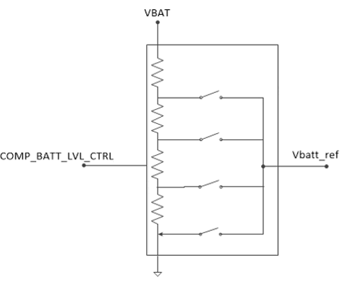
Once enabled by configuring the COMP_REG_0.WAKE_COMP_EN bit, the comparator starts to work. When the wakeup comparator module is started, V1 starts to be compared with V2 continuously. When V1 exceeds V2, the wakeup comparator will be triggered. The CHANNEL_SEL_P and CHANNEL_SEL_N fields are used to select the input of V1 and V2. When Vbatt_ref is selected in the CHANNEL_SEL_N or CHANNEL_SEL_P field. The COMP_BATT_LVL_CTRL field is used to select a level value. The following figure shows the settings of VBAT control level. The COMP_BATT_LVL_CTRL level value ranges from 0 to 7, and the calculation formula of Vbatt_ref is shown below:
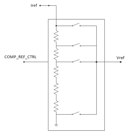
When Vref is selected in the CHANNEL_SEL_P or CHANNEL_SEL_N field. The COMP_REF_CTR field is used to select a level value. The settings of Vref control level is showed in the following figure. The COMP_REF_CTRL level value ranges from 0 to 255, and the calculation formula of Vref is shown below:
When the Vref voltage is within the range of 30 mV to 1.7 V, the actual output voltage of the Vref can closely approximate the calculated value derived from the formula above.
The selected analog pins will be acquired by the comparator once it is enabled.
Hysteresis
The configurable 52 mV (±26 mV) hysteresis could be added into the wakeup comparator, which helps ensure the slowly changing voltage or a slightly noisy voltage that will cause the comparator not to output to oscillate frequently when the two input voltages are almost close. This could increase the anti-interference ability of the comparator.
The hysteresis mode can be configured by the COMP_REG_1.NEGATIVE_HYS_EN bit and COMP_REG_1.POSITIVE_HYS_EN bit. The hysteresis on both sides mode is illustrated in the following figure. The comparator will trigger a falling edge interrupt when V1 becomes lower than V2- (VHYST/2). It will also trigger a rising edge interrupt when V1 becomes higher than V2+ (VHYST/2), VHYST is 52 mV. Here it is assumed that V1 is connected to the positive side of the comparator, and V2 is connected to the negative side of the comparator.

Res Degeneration
Res degeneration is set for calibration. The default values of the COMP_REG_1.NEGATIVE_RES_DEGENERATION field and the COMP_REG_1.POSITIVE_RES_DEGENERATION field are 0x8 and are always kept unchanged.
The COMP module obtains positive and negative res degeneration which means users can calibrate the comparator by adjusting positive and negative sides. For example, when the comparator outputs a valid signal, the voltage values at N and P sides of the comparator should be approximately equal; if it is found that the actual voltage at P side is too much higher than that at N side, you can set the value of COMP_REG_1.NEGATIVE_RES_DEGENERATION smaller, or set the value of COMP_REG_1.POSITIVE_RES_DEGENERATION larger.
CascRes Half
The COMP_REG_1.CASCRES_HALF_CTRL bit is used to ensure that the comparator is in proper operation at different bias currents.
- The COMP_REG_0.CASCRES_HALF_CTRL is set to 1 for half resistor when COMP_REG_0.ICOMP_CTRL is set to 0000.
- The COMP_REG_0.CASCRES_HALF_CTRL is set to 0 for full resistor when COMP_REG_0.ICOMP_CTRL is set to 1111.
Bias Current Set
The COMP_REG_0. ICOMP_CTRL field is used to configure the bias current. Higher bias currents will reduce the response time of the comparator, but with a corresponding increase in power consumption. Lower bias currents will increase the response time of the comparator, but with a corresponding reduce in power consumption. It is worth noting that this bias current is also from bandgap module, but this current and Iref are independent of each other and will not interfere with each other.
Glitch Remove
When the voltage reaches the threshold, the signal from the comp output will jitter because of noise interference. In order to eliminate jitter, users can specify a time by configuring the PMU_COMP_GLITCH_REMOVE.GLITCH_REMOV E_CYCLE field and the signal is considered valid if it does not change within this period of time. As the following figure shows, if the duration of the signal is less than the user set time Glitch_t, then the probability of triggering the interrupt will be greatly reduced. If the duration of the signal is larger than the user set time Glitch_t, then the interrupt will definitely be triggered.

Registers
COMP_REG_0
-
Name: Comparator Register 0
-
Description: This register includes REF_VALUE setting, COMP enablement, and channel selection.
-
Base Address: 0x4000A800
-
Offset: 0x40
-
Reset Value: 0x00000000
| Bits | Field Name | RW | Reset | Description |
|---|---|---|---|---|
23:20 |
CHANNEL_SEL_N |
WR |
0x0 |
Wakeup comparator channel N selection:
|
19:16 |
CHANNEL_SEL_P |
WR |
0x0 |
Wakeup comparator channel P selection:
|
15 |
RSVD |
R |
0x0 |
Reserved bits |
14:12 |
COMP_BATT_LVL_CTRL |
WR |
0x0 |
Changes the Vbatl based ref (Vbatl_vref):
…
|
11:8 |
ICOMP_CTRL |
WR |
0x0 |
|
7 |
WAKE_COMP_EN |
WR |
0x0 |
Enables or disables wakeup comparator.
|
6 |
CASCRES_HALF_CTRL |
WR |
0x0 |
CascRes Half:
|
5:2 |
RSVD |
R |
0x0 |
Reserved bits |
1 |
NEGATIVE_HYS_EN |
WR |
0x0 |
Hysteresis = 26 mV |
0 |
POSITIVE_HYS_EN |
WR |
0x0 |
Hysteresis = 26 mV |
COMP_REG_1
-
Name: Comparator Register 1
-
Description: This register includes res degeneration, reference source enable, CascRes Half, and Hysteresis.
-
Base Address: 0x4000A800
-
Offset: 0x44
-
Reset Value: 0x00000088
| Bits | Field Name | RW | Reset | Description |
|---|---|---|---|---|
15:8 |
COMP_REF_CTRL |
WR |
0x0 |
COMP REF CTRL (Vref) Changes the BG-based reference: Min = 0 V, Max =1.9 V (step = 7.5 mV).
|
7:4 |
NEGATIVE_RES_DEGENERATION |
WR |
0x8 |
Res degeneration N, for calibration only |
3:0 |
POSITIVE_RES_DEGENERATION |
WR |
0x8 |
Res degeneration P, for calibration only |
MCU_WAKEUP_CTRL
-
Name: MCU Wakeup Control Register of COMP
-
Description: For each bit, 0 indicates IRQ is disabled, and 1 indicates IRQ is enabled.
-
Base Address: 0x4000A000
-
Offset: 0x80
-
Reset Value: 0x0000FFFF
| Bits | Field Name | RW | Reset | Description |
|---|---|---|---|---|
6 |
COMP_FALL |
|
||
4 |
COMP_RISE |
WR |
0x1 |
|
AON_SLP_EVENT
-
Name: AON Sleep Event Register of COMP
-
Description: Events that happen in sleep or active mode, controlled by MCU_WAKE_UP_CTRL.
Note:When clearing the individual event, do not use read-mask-write but simply write ~ (1<< EVENT_BIT) to AON_SLP_EVENT.
-
Base Address: 0x4000A000
-
Offset: 0x84
-
Reset Value: 0x00000000
| Bits | Field Name | RW | Reset | Description |
|---|---|---|---|---|
6 |
COMP_FALL |
WR |
0x0 |
Write 0 to this bit to clear comp event. |
4 |
COMP_RISE |
WR |
0x0 |
Write 0 to this bit to clear comp event. |
PMU_COMP_GLITCH_REMOVE
-
Name: COMP Glitch Remove Register
-
Description: To remove voltage jitter, add deglitch circuit on comparator output (glitch: from 4 μs to 28 μs at a 4 μs step).
-
Base Address: 0x4000A000
-
Offset: 0x2C0
-
Reset Value: 0x00000000
| Bits | Field Name | RW | Reset | Description |
|---|---|---|---|---|
31:3 |
RSVD |
R |
Reserved bits |
|
2:0 |
GLITCH_REMOVE_CYCLE |
WR |
0 |
|
Electrical Specifications
In the table below, the typical values are measured at 25°C, and the minimum and maximum values are measured at the worst process and temperature conditions.
| Symbol | Description | Min. | Typ. | Max. | Unit |
|---|---|---|---|---|---|
| V_hyst | Optional hysteresis in wakeup comparator | 0 | 52 | 52 | mV |
| VREF | Optional VREF voltage in wakeup comparator | 0 | 1.89 | V | |
| VBAT_REF | Optional VBAT voltage in wakeup comparator | 0.1 * VBATL | 0.8 * VBATL | V | |
| Error_VBAT | The trigger error rate when the reference source is Vbat | 5 | % | ||
| Error_VREF | The trigger error rate when the reference source is Vref | 5 | % | ||
| Error_MSIO | The trigger error rate when the reference source is MSIO_0–MSIO_7 | 10 | mV | ||
| P_HYS | Positive hysteresis voltage in wakeup comparator | 22 | 23 | 26 | mV |
| N_HYS | Negative hysteresis voltage in wakeup comparator | 21 | 23 | 26 | mV |
