

GR5513BENDU QFN40
Figure 6 shows the pinout of GR5513BENDU QFN40 package (top view).
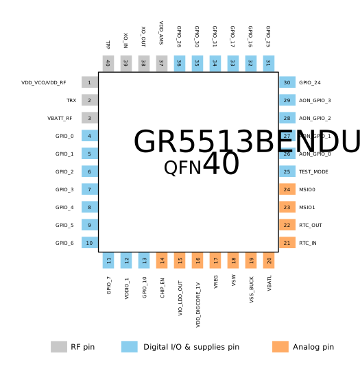
Table 6 shows pin descriptions of GR5513BENDU QFN40 package.
| Pin # | Pin Name | Pin Type | Description/Default Function | Voltage Domain |
|---|---|---|---|---|
| 1 | VDD_VCO/VDD_RF | Analog/RF supply | Synthesizer VCO supply/RF supply: 1.1 V; connect to VREG. |
|
| 2 | TRX | Analog/RF | RX input and TX output | |
| 3 | VBATT_RF | Analog/RF | Connect to VBATL. | |
| 4 | GPIO_0 | Digital I/O | General purpose I/O; default: SWD_CLK; pad drive level is 2 mA. | VDDIO1 |
| 5 | GPIO_1 | Digital I/O | General purpose I/O; default: SWD_IO; pad drive level is 2 mA. | VDDIO1 |
| 6 | GPIO_2 | Digital I/O | General purpose I/O; pad drive level is 2 mA. | VDDIO1 |
| 7 | GPIO_3 | Digital I/O | General purpose I/O; pad drive level is 2 mA. | VDDIO1 |
| 8 | GPIO_4 | Digital I/O | General purpose I/O; pad drive level is 2 mA. | VDDIO1 |
| 9 | GPIO_5 | Digital I/O | General purpose I/O; pad drive level is 2 mA. | VDDIO1 |
| 10 | GPIO_6 | Digital I/O | General purpose I/O; pad drive level is 2 mA. | VDDIO1 |
| 11 | GPIO_7 | Digital I/O | General purpose I/O; pad drive level is 2 mA. | VDDIO1 |
| 12 | VDDIO_1 | Digital I/O Supply | I/O supply voltage. Support external 1.8 V–3.3 V input voltage. | VDDIO1 |
| 13 | GPIO_10 | Digital I/O | General purpose I/O; pad drive level is 2 mA. | VDDIO1 |
| 14 | CHIP_EN | Mixed Signal IN | Master Enable for chip reset pin. The high value of CHIP_EN equals VBATL. |
|
| 15 | VIO_LDO_OUT | Analog/PMU | Output of on-chip I/O supply regulator. For GR5513BENDU, power input pin of VDDIO0 digital IO domain. When VDDIO0 is set to 3.3 V/VBATL, VIO_LDO_OUT should be connected to 3.3 V/VBATL. |
Connected internally to VDDIO0 |
| 16 | VDD_DIGCORE_1V | Analog/PMU | On-chip LDO output for digital core. Connect to a 1 µF capacitor. | |
| 17 | VREG | Analog/PMU | Feedback pin from switching regulator | |
| 18 | VSW | Analog/PMU | DC/DC converter switching node | |
| 19 | VSS_BUCK | Analog/PMU | DC/DC converter supply and general battery GND | |
| 20 | VBATL | Analog/PMU | Power supply: 2.2 V to 3.8 V | |
| 21 | RTC_IN | Analog/PMU | Input of inverting amplifier connected to 32.768 kHz crystal | |
| 22 | RTC_OUT | Analog/PMU | Output of inverting amplifier connected to 32.768 kHz crystal | |
| 23 | MSIO1 | Mixed Signal I/O | Configurable to be a GPIO mixed signal (SNSADC interface); pad drive level is 2 mA. | VBATL |
| 24 | MSIO0 | Mixed Signal I/O | Configurable to be a GPIO mixed signal (SNSADC interface); pad drive level is 2 mA. | VBATL |
| 25 | TEST_MODE | Digital I/O | Factory test mode selection pin
|
VDDIO0 |
| 26 | AON_GPIO_0 | Digital I/O | Always-on GPIO; pad drive level is 2 mA. | VDDIO0 |
| 27 | AON_GPIO_1 | Digital I/O | Always-on GPIO; pad drive level is 2 mA. | VDDIO0 |
| 28 | AON_GPIO_2 | Digital I/O | Always-on GPIO; pad drive level is 2 mA. | VDDIO0 |
| 29 | AON_GPIO_3 | Digital I/O | Always-on GPIO; pad drive level is 2 mA. | VDDIO0 |
| 30 | GPIO_24 | Digital I/O | General purpose I/O; pad drive level is 2 mA. | VDDIO0 |
| 31 | GPIO_25 | Digital I/O | General purpose I/O; pad drive level is 2 mA. | VDDIO0 |
| 32 | GPIO_16 | Digital I/O | General purpose I/O; pad drive level is 2 mA. | VDDIO0 |
| 33 | GPIO_17 | Digital I/O | General purpose I/O; pad drive level is 2 mA. | VDDIO0 |
| 34 | GPIO_31 | Digital I/O | General purpose I/O; pad drive level is 2 mA. | VDDIO0 |
| 35 | GPIO_30 | Digital I/O | General purpose I/O; pad drive level is 2 mA. | VDDIO0 |
| 36 | GPIO_26 | Digital I/O | General purpose I/O | VDDIO0 |
| 37 | VDD_AMS | Analog/RF | AMS supply 1.1 V; connect to VREG. | |
| 38 | XO_OUT | Analog/RF | Output of inverting amplifier connected to 32 MHz crystal | |
| 39 | XO_IN | Analog/RF | Input of inverting amplifier connected to 32 MHz crystal | |
| 40 | TPP | Analog/RF | Test Mux + output |