
ISO/IEC 7816-3 Master
Introduction
GR5526 SoC has one instance of SIM interface block that implements ISO/IEC 7816 standard. ISO/IEC 7816 is an international standard related to electronic identification cards with contacts, especially smart cards, managed jointly by the International Organization for Standardization (ISO) and the International Electrotechnical Commission (IEC).
Main Features
- UICC power save (clock stop)
- UICC cold and warm reset
- Guard time handling
- Wait time evaluation
- Low power design
Functional Description
The SIM interface module provides an interface to an external Universal Integrated Circuit Card (UICC) containing the Universal Subscriber Identity Module (USIM) application. The corresponding software module implements the SIM terminal transport, Card Application Toolkit (CAT), and application layer. It has a software interface to access all required USIM functions.
Block Diagram
The block diagram of SIM Interface is illustrated in 图 63. A main clock gate disables the module clock during any module inactivity for a minimal dynamic power consumption. The SIM clock is derived from the module clock and base for the Elementary Time Unit (ETU) generation. SIM clock and ETU are tracked by counters.
A shift register in the I/O module de-/serializes the bit stream and calculates/checks the parity. Data bytes are served by/to a Byte Direct Memory Access (DMA). The overall transmission is managed by the control unit. Events are signaled via interrupts. The UICC presence is monitored by the presence observer module.

Hardware Behavior
The SIM interface hardware module supports the physical, data link, and transport layer defined in ETSI TS 131 101.
Physical Layer
The SIM interface hardware module interfaces the UICC with the following ports:
- Clock (CLK)
- Reset (RST)
- Input/Output (I/O)
- UICC presence (PRE)
The detailed electrical required characteristic of the ports can be taken from ETSI TS 131 101.
CLK
The SIM clock is derived from dividing the module clock by CLK_CFG.CLK_DIV.
The SIM clock frequency shall be in the range of 1 to 5 MHz, 4 MHz during UICC initialization and 5 MHz during normal operation. The clock division has to be chosen accordingly.
RST
The UICC will be reset by the RST pin of the SIM interface module, and the RST is controlled by the register CTRL.ACTION.
I/O
The bidirectional I/O pad on chip top level is implemented as open drain with a recommended pull up to VCC of 20 kΩ. If supported by the UICC, the I/O pad can use low-impedance drivers to save power.
PRE
UICC holder often serve a card presence contact. Any card presence change will trigger an interrupt (see STAT.PRESENCE_STAT and STAT.IRQ_PRESENCE in the STAT register).
Power States
The SIM interface module is responsible for executing the cold reset, warm reset, clock stop and the power down sequence. Software triggers power state changes by writing register field CTRL. ACTION.
Activation on Cold Reset
The activation sequence and cold reset sequence is shown in 图 64. At first VCC is ramped up. With Ta the clock starts while the reset is still asserted. On Tb the reset is released and the UICC has to start with the ATR within tc.
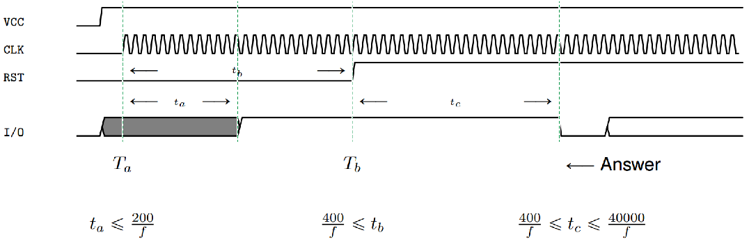
The I/O pin is not actively driven by the SIM interface during the entire cold reset procedure. The high level is ensured by the pull-up resistor. Therefore ta is not implemented in the SIM interface.
tb is hard-coded to 400 clock cycles.
The minimum tc is not checked by the SIM interface module.
The maximum tc is defined by register fields CLK_CFG.ETU_DIV and TIMES_CFG.WAIT_TIME with respect to the following equation.
The reset values are chosen according the specification to receive the ATR without any modifications. CLK_CFG.ETU_DIV is 371 and TIMES.WAITTIME is 107 (see the equation below).
If maximum tc is not met by the UICC, interrupt STAT.IRQ_RX_ERR is triggered.
Warm Reset
The warm reset sequence is shown in 图 65.
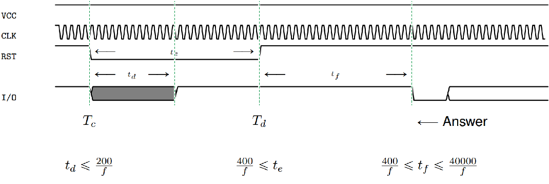
The warm reset is implemented identically to the cold reset, with Tc = Ta, Td = Tb, td = ta, te = tb and tf = tc.
Due to the fact that the registers CLK_CFG and TIMES_CFG may have changed after the ETU evaluation, the reset values have to be restored by firmware before triggering the warm reset.
Clock Stop
The clock stop sequence is shown in 图 66.
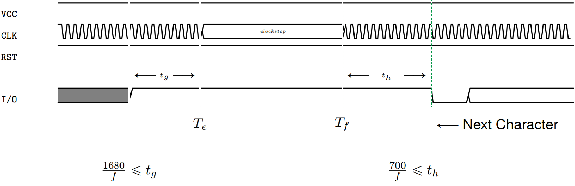
The times tg and th are ensured by the SIM interface hardware module, with and .
Deactivation
The UICC deactivation sequence is shown in 图 67.
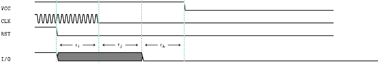
The times ti and tj are ensured by the SIM interface hardware module, with and . The timing tk depends on the VCC source.
Data Link Layer
Elementary Time Unit (ETU)
The nominal duration of one moment on the electrical circuit I/O is named Elementary Time Unit (ETU).
The ETU shall be equal to F/D clock cycles on the electrical circuit CLK where F and D are the transmission parameters. F is the clock rate conversion integer and D is the baud rate adjustment integer. F, D and f are negotiated during the initialization and setup by firmware. Possible values for F and D are shown in 表 341.
| F | D | F/D |
|---|---|---|
372 |
1 |
372 |
372 |
2 |
186 |
372 |
3 |
124 |
372 |
4 |
93 |
512 |
1 |
512 |
512 |
2 |
256 |
512 |
4 |
128 |
512 |
8 |
64 |
512 |
16 |
32 |
512 |
32 |
16 |
512 |
64 |
8 |
f is configured as described in “CLK”.
The chosen ETU has to be written to the register field CLK_CFG.ETU_DIV.
Fractional ETU values are not supported.
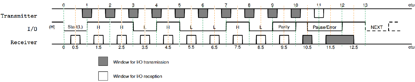
Character Frame
The character transmission timing is shown in 图 68. A character consists of:
-
Start Bit
-
Data Bits
-
Parity Bit
-
2 Stop Bits with error signaling
Error Signal and Character Repetition
- RX
In case of detected parity error during reception, the RX behavior depends on register field STAT.RX_RETRY_MAX. If the number of retries is not exceeded, the I/O pin is pulled low for one clock cycle to trigger a retransmission. Otherwise or if RETRY_MAX = 0, the received byte is discarded and the reception is aborted with a STAT.IRQ_RETRY_ERR interrupt. The internal retry counter is restarted with every character.
The maximum number of retries during the reception of one byte is displayed in register field STAT.RX_RETRY_MAX and cleared via CTRL.RX_RETYR_MC.
- TX
In case of an error signaling from the receiver, the TX behavior depends on register field STAT.TX_RETRY_MAX. If the number of retries is not exceeded, the character is retransmitted. Otherwise or if RETRY_MAX = 0, the transmission is aborted with a STAT.IRQ_RETRY_ERR interrupt. The internal retry counter is restarted with every character.
The maximum number of retries during the transmission of one byte is displayed in register field STAT.TX_RETRY_MAX and cleared via CTRL.TX_RETYR_MC.
Guard Time and Wait Time
The guard time specifies the minimum time between the leading edge of two consecutive characters, and the time has to be taken into account by the transmitter. The wait time specifies the maximum time between the leading edge of two consecutive characters, and the time has to be monitored by the receiver before issuing a timeout.
The guard time is adjusted by register field TIMES_CFG.GUARD_TIME and respected before transmitting a character. This includes the scenarios when the SIM interface has received a character and starts a transmission afterwards. The minimal guard time is 12. Register field TIMES_CFG.GUARD_TIME values smaller than that are ignored.
The wait time is adjusted by register field TIMES_CFG.WAIT_TIME and respected before aborting a character reception.
Answer to Reset
After a cold or warm reset, the UICC answers with the Answer to Reset (ATR). The module receives the ATR and decodes the first byte TS. TS marks the used encoding. If enabled in register field DATA_CFG.DETECT_CODING, the coding is set accordingly in DATA_CFG.CODING. All subsequent bytes are decoded with ISO/IEC 7816-3.
The class selection procedure and the Protocol and Parameter Select (PPS) (as a response to the ATR) procedure is controlled by firmware. After the PPS procedure, the firmware is responsible for configuring the transport protocol, clock frequency, I/O mode, and ETU.
Receive and Transmit
The SIM interface hardware module writes all received data bytes via a Byte DMA to a memory. Transmitted data bytes are read via the same Byte DMA.
Byte DMA
The Byte DMA accesses memory addresses word-wise and interacts with the I/O module on a byte base. In transmitting process, one entire word is read and served byte-wise. Irrelevant bytes are simply ignored. In receiving process, the word is cleared at the beginning and filled byte-wise. After receiving the fourth byte or after receiving the last byte, the entire word is written to the memory.
Address Ranges
Receive and transmit buffers share the same start address (register START_ADDR), which has to be aligned to 4.
The internal word address counting is limited to 18 bits. Therefore, the maximum receive and transmit buffer sizes are limited to 2(18+2) Bytes (1 MB). The buffers shall not cross a 1 MB address boundary.
Receive Buffer
The receive buffer end address is controlled by register field RX_END_ADDR and has to be calculated according to the following equation for an expected number of bytes NRX.
A done interrupt will be issued after receiving NRX bytes.
If less bytes are received and the wait time is expired, an rx_err interrupt is triggered. The register address (addr) points to the last received byte, which can be used to calculate the number of received bytes nrx.
If more bytes are served by the UICC than expected, an rx_err interrupt is triggered, but the incoming bytes are ignored and addr stays untouched.
Transmit Buffer
The transmit buffer end address is controlled by register field TX_END_ADDR and has to be calculated according to the following equation for an expected number of bytes NTX.
DMA Error
A DMA error interrupt dma_err is triggered under any of the following conditions:
-
Invalid address
-
Bus slave responses with an error
-
Word could not be read within one ETU
-
Word could not be written within one character
Action State
By default, the SIM interface hardware module does nothing, unless the firmware requests an action by writing register field CTRL.ACTION.
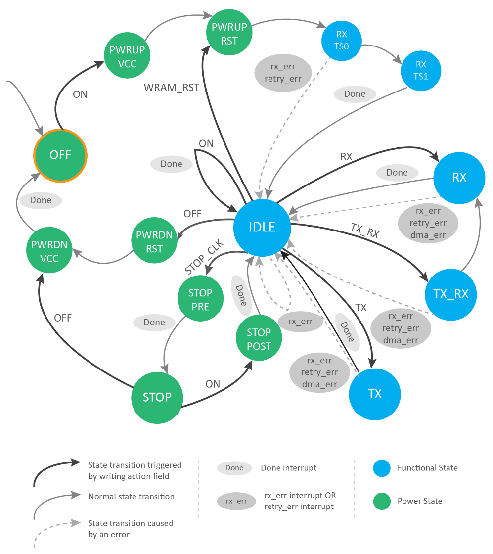
The main state machine is shown in 图 69, with the following major states:
- OFF: UICC is powered off.
- IDLE: UICC is powered on and ready to communicate.
- RX: Receive characters from UICC and store them in the receive buffer.
- TX: Read characters from the transmit buffer and transmit them to UICC.
- TX_RX: Read characters from the transmit buffer and transmit them to UICC, continue with RX.
- STOP: UICC is powered on but clock is stopped.
The main state machine operation bases on the following rules:
- The reset state is OFF.
- The action NONE (0) does nothing.
- The states OFF, IDLE, and STOP are inactive states with BUSY = 0.
- All other states are active states with BUSY = 1.
- The busy flag is visible in register field STAT.BUSY.
- It is only allowed to request the state transitions in 图 69.
- Any other action will trigger a state_err interrupt, but not abort the ongoing action.
- On entering of an inactive state a done interrupt is triggered (if no error occurs).
- In case of an rx_err, retry_err or dma_err error, the corresponding interrupt is issued, and the idle state is entered.
- Requesting ON during IDLE does nothing except triggering a done interrupt.
Transport Layer
The module supports the automatic transmission and reception of multiple bytes. With the in-built DMA the TX data is take from or the RX data is written directly into the memory. For TX, the firmware writes the payload into the memory and configures the module with payload start address and payload length. The module transfers the payload automatically and signalizes the end of the transmission with an interrupt. For RX, the firmware configures the module with expected payload length and payload address. The module writes the received payload at the configured memory address. The number of received bytes is stored inside the module and interrupts for both the beginning of transmission and end of transmission are generated.
ISO/IEC 7816-3 defines three types of data transport modes:
- Plain mode: In plain mode, the module transmits or receives multiple bytes controlled by software. Thus, the module is explicitly set in TX, RX or TX followed by RX mode.
- T = 0 mode: T = 0 mode is not implemented in hardware on purpose. SIM implementations vary in details. Therefore, the implementation is done in firmware using plain mode.
- T = 1 mode: T = 1 mode is not implemented in hardware on purpose. SIM implementations vary in details. Therefore, the implementation is done in firmware using plain mode.
Registers
CTRL
- Name: Control Register
- Description: This register is used to control the interrupts and TX/RX retries of the SIM interface module. This register is only for write purposes.
- Base Address: 0x4000F200
- Offset: 0x0
- Reset Value: 0x00000000
| Bits | Field Name | RW | Reset | Description |
|---|---|---|---|---|
31 |
IRQ_TEST_SET |
W |
0x0 |
Interrupt Test Set. This register sets test interrupt. Value:
|
30 |
IRQ_TEST_CLR |
W |
0x0 |
Interrupt Test Clear. This register clears test interrupt (has higher priority than ‘IRQ_TEST_SET’) Value:
|
29:26 |
RSVD |
W |
Reserved bits |
|
25 |
IRQ_PRESENCE_CLR |
W |
0x0 |
Interrupt source presence clear. This register clears interrupt source ‘STAT.IRQ_PRESENCE’. Value:
|
24 |
IRQ_STAT_EC |
W |
0x0 |
Interrupt source state_err clear. This register clears interrupt source ‘STAT.IRQ_STAT_ERR’. Value:
|
23 |
IRQ_DMA_EC |
W |
0x0 |
Interrupt source dma_err clear. This register clears interrupt source ‘STAT.IRQ_DMA_ERR’. Value:
|
22 |
IRQ_RETYR_EC |
W |
0x0 |
Interrupt source retry_err clear. This register clears interrupt source ‘STAT.IRQ_RETYR_ERR’. Value:
|
21 |
IRQ_RX_EC |
W |
0x0 |
Interrupt source rx_err clear. This register clears interrupt source ‘STAT.IRQ_RX_ERR’. Value:
|
20 |
IRQ_DONE_CLR |
W |
0x0 |
Interrupt source done clear. This register clears interrupt source ‘STAT.IRQ_DONE’. Value:
|
19:13 |
RSVD |
W |
Reserved bits |
|
12 |
TX_RETYR_MC |
W |
0x0 |
Transmit Retries Maximum Clear. This register clears ‘STAT.TX_RETRY_MAX’. Value:
|
11:9 |
RSVD |
W |
Reserved bits |
|
8 |
RX_RETYR_MC |
W |
0x0 |
Receive Retries Maximum Clear. This register clears ‘STAT.RX_RETRY_MAX’. Value:
|
7:3 |
RSVD |
W |
Reserved bits |
|
2:0 |
ACTION |
W |
0x0 |
Value:
|
STAT
- Name: Status Register
- Description: This register records interrupts, I/O, and power status.
- Base Address: 0x4000F200
- Offset: 0x04
- Reset Value: 0x00020000
| Bits | Field Name | RW | Reset | Description |
|---|---|---|---|---|
31 |
RSVD |
R |
Reserved bits |
|
30 |
IRQ_TEST |
R |
0x0 |
Interrupt Test. Test interrupt for connection check. Value:
|
29:26 |
RSVD |
R |
Reserved bits |
|
25 |
IRQ_PRESENCE |
R |
0x0 |
Interrupt Presence. SIM card presence changed: Inserted or removed. Value:
|
24 |
IRQ_STAT_ERR |
R |
0x0 |
Interrupt State Error. Action requested while busy or unsupported transition. Value:
|
23 |
IRQ_DMA_ERR |
R |
0x0 |
Interrupt DMA Error. DMA read/write operation could not be issued. Value:
|
22 |
IRQ_RETRY_ERR |
R |
0x0 |
Interrupt Retry Error. Maximum number of retries exceeded. Value:
|
21 |
IRQ_RX_ERR |
R |
0x0 |
Interrupt RX Error. No or incomplete or unexpected data. Value:
|
20 |
IRQ_DONE |
R |
0x0 |
Interrupt Done. Requested operation has been completed. Value:
|
19:18 |
RSVD |
R |
Reserved bits |
|
17 |
PRESENCE_STAT |
R |
0x1 |
Status of presence I/O. Value:
|
16 |
BUSY |
R |
0x0 |
Status of SIM interface. Value:
|
15 |
RSVD |
R |
Reserved bits |
|
14:12 |
TX_RETRY_MAX |
R |
0x0 |
Maximum Transmit Retries. Maximum number of seen transmit retries after error signaling by SIM. |
11 |
RSVD |
R |
Reserved bits |
|
10:8 |
RX_RETRY_MAX |
R |
0x0 |
Maximum Receive Retries. Maximum number of seen receive retries after parity error. |
7 |
RSVD |
R |
Reserved bits |
|
6:4 |
IO_STAT |
R |
0x0 |
IO States. Value:
|
3:0 |
PWR_STAT |
R |
0x0 |
Power States. Value:
|
CLK_CFG
- Name: Clock Configuration Register
- Description: This register configures clock.
- Base Address: 0x4000F200
- Offset: 0x08
- Reset Value: 0x002F0173
| Bits | Field Name | RW | Reset | Description |
|---|---|---|---|---|
31 |
CLK_STOP_SEL |
RW |
0x0 |
Clock Stop Select. Value of the clock output during stopped clock. Value:
|
30:24 |
RSVD |
R |
Reserved bits |
|
23:16 |
CLK_DIV |
RW |
0x2F |
Clock Division. Divide system clock by this value + 1. |
15:10 |
RSVD |
R |
Reserved bits |
|
9:0 |
ETU_DIV |
RW |
0x173 |
Divide SIM clock by this value + 1 to define ETU length. The reset value is the one, needed for the ATR. |
TIMES_CFG
- Name: Times Configuration Register
- Description: This register configures the timing.
- Base Address: 0x4000F200
- Offset: 0x10
- Reset Value: 0x006B0000
| Bits | Field Name | RW | Reset | Description |
|---|---|---|---|---|
31:30 |
RSVD |
R |
Reserved bits |
|
29:12 |
WAIT_TIME |
RW |
0x6B |
Wait time in [ETU]. Maximum card response time (leading edge to leading edge). |
11:10 |
RSVD |
R |
Reserved bits |
|
9:0 |
GUARD_TIME |
RW |
0x0 |
Guard time in [ETU]. Time between the leading edges of two consecutive characters. |
DATA_CFG
- Name: Data Configuration Register
- Description: This register configures the communication.
- Base Address: 0x4000F200
- Offset: 0x14
- Reset Value: 0x00000002
| Bits | Field Name | RW | Reset | Description |
|---|---|---|---|---|
31:7 |
RSVD |
R |
Reserved bits |
|
6:4 |
RETRY_LIMIT |
RW |
0x0 |
Retries Limit. Maximum number of issued retries before giving up. |
3:2 |
RSVD |
R |
Reserved bits |
|
1 |
DETECT_CODING |
RW |
0x1 |
Detect Coding Convention. Automatically detect coding convention during ATR reception. Value:
|
0 |
CODING |
RW |
0x0 |
Coding Convention. Value:
|
ADDR
- Name: Address Register
- Description: This register records current address relative to base_addr.
- Base Address: 0x4000F200
- Offset: 0x18
- Reset Value: 0x00000000
| Bits | Field Name | RW | Reset | Description |
|---|---|---|---|---|
31:20 |
RSVD |
R |
Reserved bits |
|
19:2 |
ADDR |
R |
0x0 |
Address. Current address relative to base_addr. |
1:0 |
ADDR_FRAC |
R |
0x0 |
Address Fraction. Byte selection. |
START_ADDR
- Name: Start Address Register
- Description: This register configures read/write memory address. RX and TX buffers have to be aligned to 4 bytes, and buffer address [31:2] = START_ADDR[31:2]
- Base Address: 0x4000F200
- Offset: 0x1c
- Reset Value: 0x00000000
| Bits | Field Name | RW | Reset | Description |
|---|---|---|---|---|
31:20 |
BASE_ADDR |
RW |
0x0 |
Base Address. Base Address for RX and TX buffers. |
19:2 |
START_ADDR |
RW |
0x0 |
Start Address. Start address of RX and TX buffers, relative to base_addr. |
1:0 |
RSVD |
R |
Reserved bits |
RX_END_ADDR
Name: RX End Register
Description: This register configures RX data end address.
Base Address: 0x4000F200
Offset: 0x20
Reset Value: 0x00000000
| Bits | Field Name | RW | Reset | Description |
|---|---|---|---|---|
31:20 |
RSVD |
R |
Reserved bits |
|
19:2 |
RX_END_ADDR |
RW |
0x0 |
RX End Address. End address of receive buffer, relative to base_addr. |
1:0 |
RX_END_AF |
RW |
0x0 |
RX End Address Fraction. Byte selection. |
TX_END_ADDR
Name: TX End Register
Description: This register configures TX data end address.
Base Address: 0x4000F200
Offset: 0x24
Reset Value: 0x00000000
| Bits | Field Name | RW | Reset | Description |
|---|---|---|---|---|
31:20 |
RSVD |
R |
Reserved bits |
|
19:2 |
TX_END_ADDR |
R |
0x0 |
TX End Address. End address of transmit buffer, relative to base_addr. |
1:0 |
TX_END_AF |
R |
0x0 |
TX End Address Fraction. Byte selection. |
Electrical Specifications
| Symbol | Description | Min. | Typ. | Max. | Unit |
|---|---|---|---|---|---|
fSIMCLK |
UICC CLK frequency |
1 |
5 |
MHz |
|
VCC |
UICC Voltage class supported |
1.8 |
3.08 |
V |
