PDM
Introduction
The Pulse Density Modulation (PDM) module provides 1 instance and 2 channels for external audio front ends, for example, digital microphones. It also supports DMA for data transfer.
Main Features
- 1 instance
- 2 channels
- Left channel: Collect data on the rising edge.
- Right channel: Collect data on the failing edge.
- Up to two PDM microphones configured as a left/right pair using the same data input
- Supporting 8 kHz, 15.625 kHz, and 16 kHz sampling rates
- 16-bit samples
- Hardware decimation filters
- DMA support
- Programmable gain control
Block Diagram
The functional block diagram of PDM is shown in 图 125. The PDM module comprises DMIC Chain Left, DMIC Chain Right, and PDM Register Block.

Protocols Introduction
PDM module is an interface for PDM signal input to PCM audio format output, so the input is 1-bit data in PDM format, and the output data is in PCM format.
Protocols Introduction
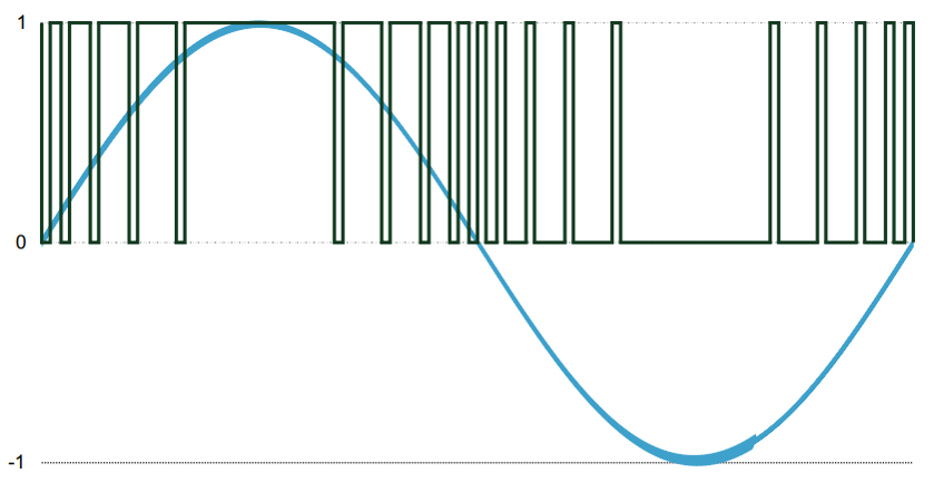
PDM is a modulation method that uses digital signals to represent analog signals. There is only 1-bit output, and non-zero is 1, so digital audio represented by PDM is also called oversampled 1-bit Audio. It is a high-frequency data stream of 1-bit digital sampling. In a PDM signal, the relative density of the pulse corresponds to the amplitude of the analog signal. As shown below, a large number of “1s” corresponds to high (positive) amplitude values, and a large number of “0s” corresponds to low (negative) amplitude values; alternating “1s” and “0s” corresponds to amplitude values.
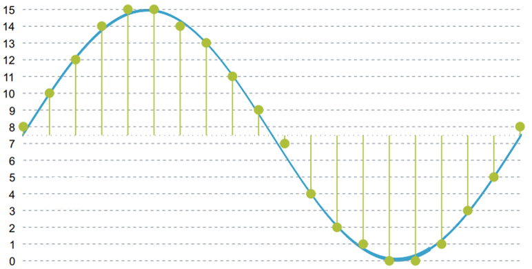
PCM Introduction
In the PCM (Pulse Code Modulation) signal, the specific amplitude value is encoded as a pulse. The PCM stream has two basic properties which determine the fidelity of the stream relative to the original analog signal.
- Sampling rate
- Bit depth
Sampling rate is used to represent the signal digitally, the number of signal samples collected per second. The bit depth determines the number of bits of information in each sample.
Functional Description
The PDM module of GR5526 supports single-channel and dual-channel operating modes. It has two wires – serial data in (DI) and serial clock (CLOCK).
PDM Pin Mux
Before configuring the PDM module functions, make sure the pin mux of PDM interface GPIO is configured as PDM_CLKO and PDM_DI.
PDM Operation
By default, the left channel collects data on the rising edge of the clock, and the right channel collects data on the falling edge of the clock, resulting in two bit streams. In order to convert 1-bit data of PDM entrance into PCM audio samples, a decimation filter is included in the PDM module. The input of the filter is the two-channel PDM serial stream (with the left channel on clock high and the right channel on clock low). The output is 2 × 16-bit PCM samples at a sampling rate 64 times lower than the PDM clock rate.
PDM Gain
PDM module supports programmable gain control. The gain is controlled by the PGA_CFG_LEFT and PGA_CFG_RIGHT registers. PGA_CFG_LEFT controls the gain of the left channel, and PGA_CFG_RIGHT controls the gain of the right channel.
The control bit is a u4.10. This means it is a 14-bit unsigned number with 4 integer bits and 10 fractional bits. 0x400 gain is 0 dB, shift left by one bit approximately equal to +6dB; otherwise, shift right by one bit approximately equal to -6dB. For example, 0x800 = +6 dB and 0x200 = -6 dB. The conversion formula is as follows:
Where, X is the register value.
Some calculated values are given below:
| Value (HEX) | Gain (dB) | Value (HEX) | Gain (dB) |
|---|---|---|---|
| 00000000000001(0x01) |
-60.2 |
00000100011111(0x11F) |
-11.0 |
| 00000000000010(0x02) |
-54.2 |
00000101000010(0x142) |
-10.0 |
| 00000000000011(0x03) |
-50.7 |
00000101101010(0x16A) |
-9.0 |
| 00000000000100(0x04) |
-48.2 |
00000110010110(0x196) |
-8.0 |
| 00000000000101(0x05) |
-46.2 |
00000111000111(0x1C7) |
-7.0 |
| 00000000000110(0x06) |
-44.6 |
00000111111111(0x1FF) |
-6.0 |
| 00000000000111(0x07) |
-43.3 |
00001000111101(0x23D) |
-5.0 |
| 00000000001000(0x08) |
-42.1 |
00001010000011(0x283) |
-4.0 |
| 00000000001001(0x09) |
-41.1 |
00001011010001(0x2D1) |
-3.0 |
| 00000000001010(0x0A) |
-40.2 |
00001100101001(0x329) |
-2.0 |
| 00000000001011(0x0B) |
-39.4 |
00001110001100(0x38C) |
-1.0 |
| 00000000001100(0x0C) |
-38.6 |
00010000000000(0x400) |
0.0 |
| 00000000001110(0x0E) |
-37.3 |
00010001110111(0x477) |
1.0 |
| 00000000010000(0x10) |
-36.1 |
00010100000010(0x502) |
2.0 |
| 00000000010010(0x12) |
-35.1 |
00010110011111(0x59F) |
3.0 |
| 00000000010100(0x14) |
-34.2 |
00011001001110(0x64E) |
4.0 |
| 00000000010111(0x17) |
-33.0 |
00011100010011(0x713) |
5.0 |
| 00000000011001(0x19) |
-32.2 |
00011111110000(0x7F0) |
6.0 |
| 00000000011101(0x1D) |
-31.0 |
00100011101000(0x8E8) |
7.0 |
| 00000000100000(0x20) |
-30.1 |
00100111111110(0x9FE) |
8.0 |
| 00000000100100(0x24) |
-29.1 |
00101010010101(0xA95) |
8.5 |
| 00000000101001(0x29) |
-28.0 |
00101100110110(0xB36) |
9.0 |
| 00000000101110(0x2E) |
-27.0 |
00110010010100(0xC94) |
10.0 |
| 00000000110011(0x33) |
-26.1 |
00111000011101(0xE1D) |
11.0 |
| 00000000111001(0x39) |
-25.1 |
00111111010110(0xFD6) |
12.0 |
| 00000001000000(0x40) |
-24.1 |
01000111000100(0x11C4) |
13.0 |
| 00000001001000(0x48) |
-23.1 |
01001111101111(0x13EF) |
14.0 |
| 00000001010001(0x51) |
-22.0 |
01011001011110(0x165E) |
15.0 |
| 00000001011011(0x5B) |
-21.0 |
01100100011000(0x1918) |
16.0 |
| 00000001100110(0x66) |
-20.0 |
01110000101000(0x1C28) |
17.0 |
| 00000001110011(0x73) |
-19.0 |
01111110011000(0x1F98) |
18.0 |
| 00000010000001(0x81) |
-18.0 |
10001101110011(0x2373) |
19.0 |
| 00000010010000(0x90) |
-17.0 |
10011111000110(0x27C6) |
20.0 |
| 00000010100010(0xA2) |
-16.0 |
10110010100000(0x2CA0) |
21.0 |
| 00000010110110(0xB6) |
-15.0 |
11001000010010(0x3212) |
22.0 |
| 00000011001100(0xCC) |
-14.0 |
11100000101110(0x382E) |
23.0 |
| 00000011100100(0Xe4) |
-13.0 |
11111100001001(0x3F09) |
24.0 |
| 00000100000000(0x100) |
-12.0 |
PDM Enable
The PDM starts data sampling after the EN_LEFT/EN_RIGHT register and CLK registers have been written. When starting the module, it will take some time for the filters to start outputting valid data. Transients from the PDM microphone itself may also occur. The first few samples might hence contain invalid values or transients. It is therefore advised to discard the first few samples after a PDM start.
PDM Interrupt
The PDM module has two interrupts for the left and right channels respectively. One is the valid data interrupt, which will be generated when the PDM outputs data. The other is the data overflow interrupt, which will be generated when the DMA does not remove the data in time. The INT_LEFT/INT_RIGHT register can mask interrupts. The DATA_LEFT/DATA_RIGHT register can check interrupt flag.
PDM DMA
The PDM module supports one DMA channel for PDM transmit. It can carry data from three places: DATA_LEFT register, DATA_RIGHT register, and DATA register. The lower 16 bits of the DATA_LEFT register store the data of the left channel, and the lower 16 bits of the DATA_RIGHT register store the data of the right channel. The lower 16 bits of the DATA register store the left channel data, and the upper 16 bits store the right channel data. They are equivalent to the data of DATA_LEFT and DATA_RIGHT.
Since the PDM module does not have an internal FIFO, it is necessary to ensure the efficiency of the DMA as much as possible in the PDM DMA mode; otherwise the PDM is prone to overflow.
Hardware Connection Example
The PDM module is applicable to microphone voice acquisition. Connect the microphone clock to CLK, and data to DIN. The module supports three connection methods: left channel sample, right channel sample, and stereo sample, as shown below:

Registers
EN_LEFT
- Name: Left PDM Enable Register
- Description: This register specifies the sampling enable bit of the left channel.
- Base Address: 0x4000F700
- Offset: 0x0
- Reset Value: 0x00000000
| Bits | Field Name | RW | Reset | Description |
|---|---|---|---|---|
31:2 |
RSVD |
R |
Reserved bits |
|
1 |
SAMPLE_DMIC |
RW |
0x0 |
Left channel sampling data
|
0 |
EN_RX |
RW |
0x0 |
Left channel reset
|
PGA_CFG_LEFT
- Name: Left Channel Gain Register
- Description: This register specifies the gain of the left channel.
- Base Address: 0x4000F700
- Offset: 0x10
- Reset Value: 0x00000400
| Bits | Field Name | RW | Reset | Description |
|---|---|---|---|---|
31:14 |
RSVD |
R |
Reserved bits |
|
0:13 |
VAL |
RW |
0x400 |
Left channel gain: It is a u4.10. This means it is a 14-bit unsigned number with 4 integer bits and 10 fractional bits. 0x400 gain is 0 dB, shift left by one bit (plus 3 dB); otherwise, shift right by one bit (minus 3 dB). |
DATA_LEFT
- Name: Left Channel Data Register
- Description: This register specifies the data of the left channel.
- Base Address: 0x4000F700
- Offset: 0x14
- Reset Value: 0x00000000
| Bits | Field Name | RW | Reset | Description |
|---|---|---|---|---|
31:19 |
RSVD |
R |
0x0 |
Reserved bits |
18 |
MASK |
RW |
0x0 |
Write 1 to mask dma_req. |
17 |
OVER |
RW |
0x0 |
Left channel data overflow flag. If DMA does not read this register or combined data register before another sample is written, this bit gets asserted. Moreover, the bit can be used as an interrupt to MCU. Write a 1 to clear. |
16 |
VALID |
R |
0x0 |
Left channel data valid flag, also can be used as an interrupt to MCU. Read to clear. |
15:0 |
DATA |
R |
0x0 |
Left channel data |
INT_LEFT
- Name: Left Channel Interrupt Register
- Description: This register specifies the interrupt of the left channel.
- Base Address: 0x4000F700
- Offset: 0x18
- Reset Value: 0x00000001
| Bits | Field Name | RW | Reset | Description |
|---|---|---|---|---|
31:2 |
RSVD |
R |
0x0 |
Reserved bits |
1 |
OVER_MASK |
RW |
0x0 |
Left channel data overflow interrupt. Write 1 to mask the interrupt. |
0 |
VALID_MASK |
RW |
0x1 |
Left channel data valid interrupt. Write 1 to mask the interrupt. |
EN_RIGHT
- Name: Right PDM Enable Register
- Description: This register specifies the sampling enable bit of the right channel.
- Base Address: 0x4000F700
- Offset: 0x1C
- Reset Value: 0x00000000
| Bits | Field Name | RW | Reset | Description |
|---|---|---|---|---|
Bits |
Field Name |
RW |
Reset |
Description |
31:2 |
RSVD |
R |
Reserved bits |
|
1 |
SAMPLE_DMIC |
RW |
0x0 |
Right channel sampling data
|
0 |
EN_RX |
RW |
0x0 |
Right channel reset
|
PGA_CFG_RIGHT
- Name: Right Channel Gain Register
- Description: This register specifies the gain of the right channel.
- Base Address: 0x4000F700
- Offset: 0x44
- Reset Value: 0x00000400
| Bits | Field Name | RW | Reset | Description |
|---|---|---|---|---|
31:14 |
RSVD |
R |
Reserved bits |
|
0:13 |
VAL |
RW |
0x400 |
Right channel gain: It is a u4.10. This means it is a 14-bit unsigned number with 4 integer bits and 10 fractional bits. 0x400 gain is 0dB, shift left by one bit (plus 3 dB), otherwise, shift right by one bit (minus 3dB). |
DATA_RIGHT
- Name: Right Channel Data Register
- Description: This register specifies the data of the right channel.
- Base Address: 0x4000F700
- Offset: 0x48
- Reset Value: 0x00000000
| Bits | Field Name | RW | Reset | Description |
|---|---|---|---|---|
31:19 |
RSVD |
R |
0x0 |
Reserved bits |
18 |
MASK |
RW |
0x0 |
Write 1 to mask dma_req. |
17 |
OVER |
RW |
0x0 |
Right channel data overflow flag. If DMA does not read this register or combined data register before another sample is written, this bit gets asserted. Moreover, this bit can be used as an interrupt to MCU. Write a 1 to clear. |
16 |
VALID |
R |
0x0 |
Right channel data valid flag, also can be used as an interrupt to MCU. Read to clear. |
0:15 |
DATA |
R |
0x0 |
Right channel data |
INT_RIGHT
- Name: Right Channel Interrupt Register
- Description: This register specifies the interrupt of the right channel.
- Base Address: 0x4000F700
- Offset: 0x4C
- Reset Value: 0x00000001
| Bits | Field Name | RW | Reset | Description |
|---|---|---|---|---|
31:2 |
RSVD |
R |
0x0 |
Reserved bits |
1 |
OVER_MASK |
RW |
0x0 |
Right channel data overflow interrupt. Write 1 to mask the interrupt. |
0 |
VALID_MASK |
RW |
0x1 |
Right channel data valid interrupt. Write 1 to mask the interrupt. |
DATA
- Name: Data Register
- Description: This specifies the Data Register.
- Base Address: 0x4000F700
- Offset: 0x50
- Reset Value: 0x00000000
| Bits | Field Name | RW | Reset | Description |
|---|---|---|---|---|
31:16 |
DATA_R |
R |
0x0 |
Right channel data, consistent with DATA_RIGHT register |
15:0 |
DATA_L |
R |
0x0 |
Left channel data, consistent with DATA_LEFT register |
CLK
- Name: CLK Enable Register
- Description: This specifies the CLK Enable Register.
- Base Address: 0x4000F700
- Offset: 0x58
- Reset Value: 0x00000000
| Bits | Field Name | RW | Reset | Description |
|---|---|---|---|---|
31:1 |
RSVD |
R |
0x0 |
Reserved bits |
9:8 |
SAMPLE_RATE |
RW |
0x1 |
PDM sampling rate.
|
0 |
EN |
R |
0x0 |
PDM CLK enable bit |
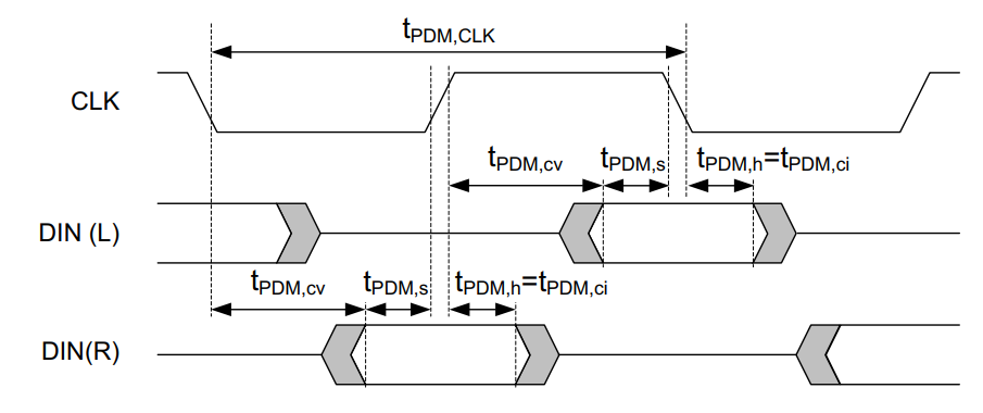
Electrical Specifications
| Symbol | Description | Min. | Typ. | Max. | Unit |
|---|---|---|---|---|---|
fPdm,clk,64 |
PDM clock speed |
1 |
M |
||
tPDM,JITTER |
Jitter in PDM clock output |
20 |
ns |
||
tPDM,DATA |
Decimation filter delay |
6.125 |
ms |
||
tPDM,cv |
Allowed clock edge to data valid |
56 |
ns |
||
tPDM,ci |
Allowed (other) clock edge to data invalid |
49 |
ns |
||
tPDM,s |
Data setup time at fPDM,CLK = 1 MHz |
65 |
ns |
||
tPDM,h |
Data hold time at fPDM,CLK = 1 MHz |
0 |
ns |
||
GPDM,default |
Default (reset) absolute gain of the PDM module |
0 |
dB |
The PDM timing diagram is as below: