DC
Introduction
The display control (DC) module is a powerful display controller which contains several smart tools and functionalities to compose multiple graphics layers by improving image quality and contributing significantly to the reduction of the SoC power consumption. The DC module supports composition features, a wide range of display interfaces, and advanced proprietary framebuffer compression technology. The core is designed to lift the workload off the Graphics Processing Unit (GPU) or the host processor (CPU), in GPU-less systems, and minimize the memory bandwidth.
Main Features
- 1 instance
- Supporting up to two layers with blending capabilities
- Programmable display resolutions up to 454 x 454
- Compressed framebuffer support
- Powerful composition
- Alpha blending
- Programmable size, offset, and format per layer
- Programmable stride/pitch enabling panning and clipping
- SPI3/SPI4/DualSPI/QuadSPI display interface
- DMA support (internal dedicated DMA)
- Input color formats: GBA-8888, ARGB-8888, ABGR-8888, BGRA-8888, RGB-888, RGBA-5551, RGB-565, RGB-332, RGB-565, TSC4,TSC6, TSC6a
- 3/4w SPI: RGB-111, RGB-332, RGB-444, RGB-565, RGB-666, RGB-888
- Dual/Quad SPI: RGB-444, RGB-565, RGB-666, RGB-888
Block Diagram
The functional block diagram of display control is shown in 图 82. The display control module contains timing generator, master arbiter, two layers, formatting block, and more.

Functional Description
Pin Mux
Before configuring the display control module functions, you must ensure that the pin mux of the display control interface GPIOs should be configured as DC_DCX, DC_CS_N, DC_CLK, DC_IO_0, DC_IO_1, DC_IO_2, and DC_IO_3.
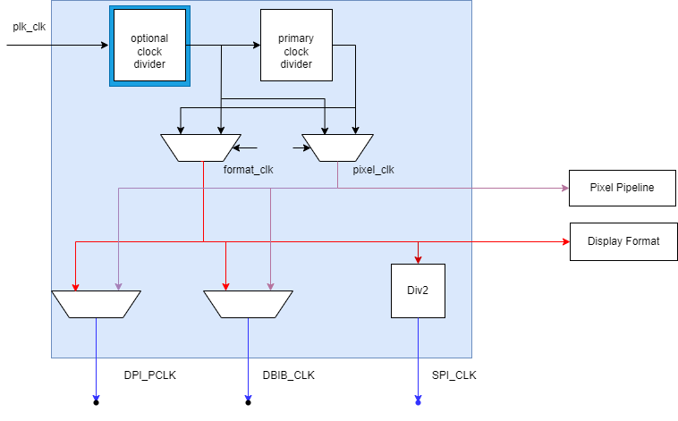
Clock Divider
The input PLL clock (pll_clk) which is serial clock is fed to the clock divider module. If the optional divider is enabled, then its input is driven by the PLL clock and its ratio is determined by the CLK_CTRL[31:27] register bits. Primary clock’s divider input is driven by the optional divider output, if it is enabled; otherwise by the PLL clock. Primary clock’s divider ratio is determined by the CLK_CTRL[5:0] register bits. In case that SPI interface is selected, the SPI_SCLK is generated by the format_clk, and then a hard division between the SPI_SCLK and the format_clk is applied depending on the INTERFACE_CFG[10:9]. The format_clk and pixel_clk are also fed to Pixel Pipeline and Display Format, representing the different processing stages of the Display controller.
Layer Overlays
The DC module supports two layers (n = 0, 1) sourced from different memory regions. Each layer can have separate color modes, alpha blending, and filtering attributes. The main control registers for each layer are the LAYERn_MODE (n = 0–1) registers. Layer 0 is on top of the background color, and Layer 1 is on top of Layer 0.
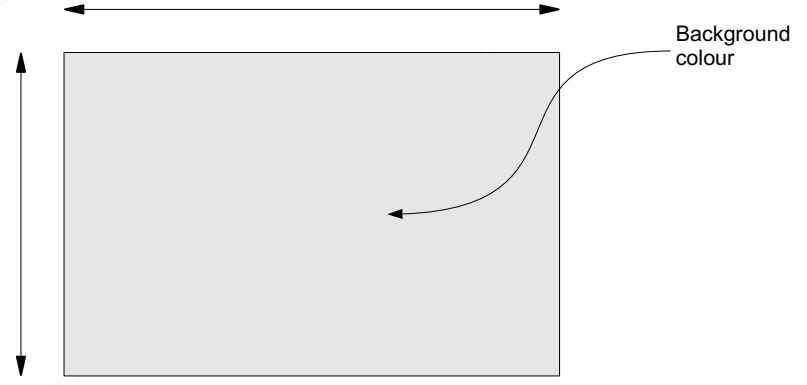
Layering starts with a 32-bit background color (RGBA), as shown in 图 84, which is applied on the entire screen. If it is not needed, the background register BG_COLOR field is set to 0. If no layer is enabled, only the background color will be displayed.
The base frame address is set in the LAYERn_BASEADDR (n = 0–1) registers. When the video image is stored in the memory, the frame buffer may contain extra bytes after each row of pixels. The number of bytes from one row of pixels to the next row in memory is called stride. These bytes affect how the image is stored in memory and the LAYERn_STRIDE[15:0] (n = 0–1) bits are used to add space between frame lines.
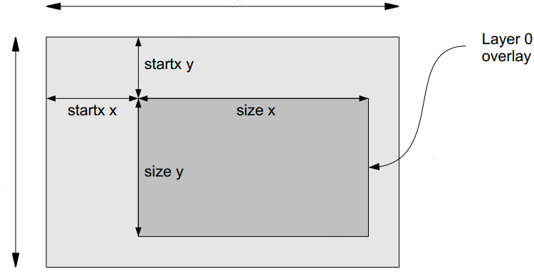
For each layer, the start location (registers LAYERn_STARTXY n = 0–1), the visible size (registers LAYERn_SIZEXY n= 0–1), and the resolution (registers LAYERn_RESXY n = 0–1) are needed. For example, if the resolution of an image is 800 x 600 and the size of the required image for layer 0 is 400 x 300 at location (68, 32), then the value of the registers are shown in 表 419:
| Parameter | Register | Register Bits | Value |
|---|---|---|---|
Resolution X |
RESXY |
31–16 |
800 |
Resolution Y |
RESXY |
15–0 |
600 |
Start coordinate X |
LAYER0_STARTXY |
31–16 |
68 |
Start coordinate Y |
LAYER0_STARTXY |
15–0 |
32 |
Pixel size in X coordinate |
LAYER0_SIZEXY |
31–16 |
400 |
Pixel size in Y coordinate |
LAYER0_SIZEXY |
15–0 |
300 |
Blending Modes
Each layer supports alpha blending. During blending process, a translucent foreground color (current layer) with a background color (previous layer) are combined, and a new blended color is produced. Foreground color’s translucency may range from completely transparent to completely opaque. If the foreground color is completely transparent, the blended color will be the background color; if the foreground color is completely opaque, the blended color will be the foreground color. When the translucency ranges in between, the blended color is computed as a weighted average of the foreground and background colors. Each layer is blended on top of the previous generated blended layer based on the following equation:
表 420 shows the blending modes that the DC module supports:
| Binary | Blending Mode | Fs | Fd |
|---|---|---|---|
| 0000 |
Blend black |
0 |
0 |
| 0001 |
Blend white |
1 |
1 |
| 0010 |
Blend alpha source |
as |
as |
| 0011 |
Blend alpha global |
ag |
ag |
| 0100 |
Blend alpha source and alpha global |
as* ag |
as* ag |
| 0101 |
Blend inverted source |
1 – as |
1 – as |
| 0110 |
Blend inverted global |
1 – ag |
1 – ag |
| 0111 |
Blend inverted source and inverted global |
1 – ( as* ag) |
1 – ( as* ag) |
| 1010 |
Blend alpha destination |
ad |
ad |
| 1101 |
Blend inverted destination |
1 – ad |
1 – ad |
as: The A channel of the source image, representing the transparency of the source image
as: The A channel of the destination image, representing the transparency of the destination image
ag: The global A channel
TSC Format
The DC’s framebuffer compression operates in screen blocks (4 x 4 pixel blocks), and depending on the configuration achieves TSC™4, TSC™6, and TSC™6a lossy, fixed-ratio compression.
• TSC™4 is a 6:1 compression (4bpp).
• TSC™6 is a 4:1 compression (6bpp).
• TSC™6a is a 4:1 compression (6bpp) with alpha channel.
Compression is performed at run time using minimal hardware. Pixel data can be stored in the framebuffer in compressed form and decompressed in the DC module. 图 86 shows the TS compression operation. The output of the TSC™4 compression is 64 bits per 4 x 4 block of pixels, and the output of the TSC™6 compression is 96 bits per 4 x 4 block of pixels. It should be noted that the three compression formats of TSC are all lossy compression, and users need to measure whether the format meets their requirements for reduction.

Display Interface
The DC module supports one-/multiple-line SPI. All supported formats are listed as follows:
- 3-wire SPI
- 4-wire SPI
- Dual SPI
- Quad SPI
The SPI serial interface is mainly composed of five parts:
- SPI_DC: data/command indicator
- SPI_CS: chip enable
- SPI_SCLK: serial clock
- SPI_SD/SPI_SD1/SPI_SD2/SPI_SD3: serial data output
- SPI_SI: serial data input

SPI 3-Wire/4-Wire Serial Interface
The SPI 3-wire serial interface uses the SPI_CS (chip enable), SPI_SCLK (serial clock), and SPI_SD (serial data output). The command word consists of 9 bits: 1-bit data/command indicator and 8-bit command. The data word consists of 1-bit data/command indicator and as many bits as required from the chosen format. The MSB is transmitted first.
The SPI 4-wire serial interface uses SPI_CS (chip enable), SPI_SCLK (serial clock), SPI_SD (serial data output), and one additional signal SPI_DC (data/command indicator). The command consists of 8 bits. The data consists of n bits, according to the chosen format. The MSB is transmitted first.
The waveform of the read data is as follows:
DualSPI Serial Interface
The DualSPI serial interface uses SPI_CS (chip enable), SPI_SCLK (serial clock), and SPI_SD & SPI_SD1 (serial data outputs). The command word is always transmitted through the SPI_SD line, and the data is routed through the SPI_SD and SPI_SD1 lines. The command word consists of 9 bits: 1-bit data/command indicator and 8-bit command. The data word consists of 1-bit data/command indicator and n bits, according to the chosen format.
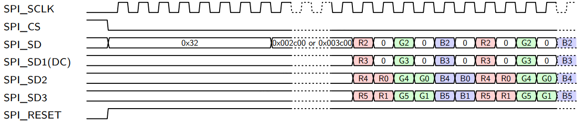
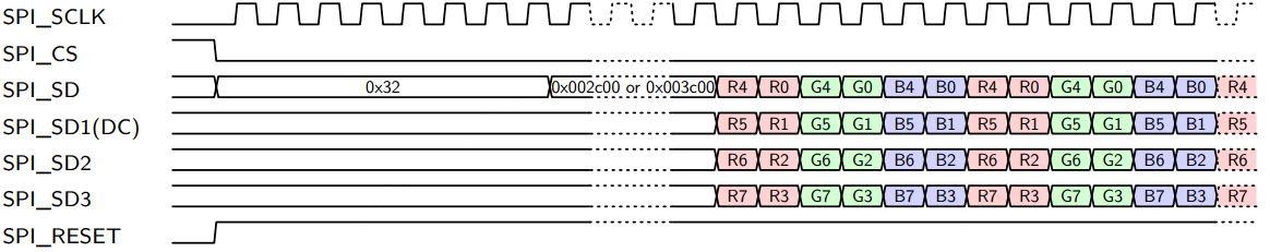
QuadSPI Serial Interface
The QuadSPI serial interface uses SPI_CS (chip enable), SPI_SCLK (serial clock), as well as SPI_SD, SPI_SD1, SPI_SD2, and SPI_SD3 (serial data outputs). The header and the command type are always transmitted through the SPI_SD line, and the data is routed through the SPI_SD, SPI_SD1, SPI_SD2, and SPI_SD3 lines. The header consists of 8 bits. The command word consists of 24 bits, and the data consists of n bits according to the chosen format.
The available signals of the SPI3/4, DualSPI, and QuadSPI interfaces are shown in the table below.
| Pin Name | Type | Description | Source |
|---|---|---|---|
| SCLK | Output | Serial clock signal | Display Controller |
| CS | Output | Chip enable when low | Display Controller |
| DC | Output | Data/Command select | Display Controller |
| SD0 | Output | Serial data | Display Controller |
| SD1 | Output | Serial data | Display Controller |
| SD2 | Output | Serial data | Display Controller |
| SD3 | Output | Serial data | Display Controller |
| SI | Input | Serial data (Read) | Display Controller |
| RESET | Output | Reset display | GPIO |
| TE | Input | Display Tearing effect signal | GPIO |
| Backlight | Output | LED driver signals | GPIO |
Color Input Format
The DC module supports multiple color formats. The supported color formats are the following:
- L1 big-endian 1-bit
表 422 L1 big-endian 1-bit Pixel 0 Pixel 1 Pixel 2 Pixel 3 Pixel 4 Pixel 5 Pixel 6 Pixel 7 7
6
5
4
3
2
1
0
L0
L0
L0
L0
L0
L0
L0
L0
Byte 0
- L4 big-endian 4-bit
表 423 L4 big-endian 4-bit Pixel 0 Pixel 1 7
6
5
4
3
2
1
0
L3
L2
L1
L0
L3
L2
L1
L0
Byte 0
- L8 8-bit
表 424 L8 8-bit Pixel 0 7
6
5
4
3
2
1
0
L7
L6
L5
L4
L3
L2
L1
L0
Byte 0
- RGBA 8888 32-bit
表 425 RGBA 8888 32-bit Pixel 0 31
30
29
28
27
26
25
24
23
22
21
20
19
18
17
16
15
14
13
12
11
10
9
8
7
6
5
4
3
2
1
0
A7
A6
A5
A4
A3
A2
A1
A0
B7
B6
B5
B4
B3
B2
B1
B0
G7
G6
G5
G4
G3
G2
G1
G1
R7
R6
R5
R4
R3
R2
R1
R0
Byte 3
Byte 2
Byte 1
Byte 0
- ARGB 8888 32-bit
表 426 ARGB 8888 32-bit Pixel 0 31
30
29
28
27
26
25
24
23
22
21
20
19
18
17
16
15
14
13
12
11
10
9
8
7
6
5
4
3
2
1
0
B7
B6
B5
B4
B3
B2
B1
B0
G7
G6
G5
G4
G3
G2
G1
G1
R7
R6
R5
R4
R3
R2
R1
R0
A7
A6
A5
A4
A3
A2
A1
A0
Byte 3
Byte 2
Byte 1
Byte 0
- ABGR 8888 32-bit
表 427 ABGR 8888 32-bit Pix 0 31 30 29 28 27 26 25 24 23 22 21 20 19 18 17 16 15 14 13 12 11 10 9 8 7 6 5 4 3 2 1 0 R7 R6 R5 R4 R3 R2 R1 R0 G7 G6 G5 G4 G3 G2 G1 G1 B7 B6 B5 B4 B3 B2 B1 B0 A7 A6 A5 A4 A3 A2 A1 A0 Byte 3 Byte 2 Byte 1 Byte 0 - BGRA 8888 32-bit
表 428 BGRA 8888 32-bit Pixel 0 31
30
29
28
27
26
25
24
23
22
21
20
19
18
17
16
15
14
13
12
11
10
9
8
7
6
5
4
3
2
1
0
A7
A6
A5
A4
A3
A2
A1
A0
R7
R6
R5
R4
R3
R2
R1
R0
G7
G6
G5
G4
G3
G2
G1
G1
B7
B6
B5
B4
B3
B2
B1
B0
Byte 3
Byte 2
Byte 1
Byte 0
- RGBA 5551 16-bit
表 429 RGBA 5551 16-bit Pixel 0 15
14
13
12
11
10
9
8
7
6
5
4
3
2
1
0
R4
R3
R2
R1
R0
G4
G3
G2
G1
G1
B4
B3
B2
B1
B0
A0
Byte 1
Byte 0
- RGBA 565 16-bit
表 430 RGBA 565 16-bit Pixel 0 15
14
13
12
11
10
9
8
7
6
5
4
3
2
1
0
R4
R3
R2
R1
R0
G5
G4
G3
G2
G1
G1
B4
B3
B2
B1
B0
Byte 1
Byte 0
- RGB 332 8-bit
表 431 RGB 332 8-bit Pixel 0 7
6
5
4
3
2
1
0
R2
R1
R0
G2
G1
G0
B1
B0
Byte 0
- TSC4 16-pixel/64-bit
表 432 TSC4 16-pixel/64-bit Pixel 15 – Pixel 0 63
62
…
…
1
0
Byte 8 – Byte 0
- TSC6 16-pixel/96-bit
表 433 TSC6 16-pixel/96-bit Pixel 15 – Pixel 0 95
94
…
…
1
0
Byte 12 – Byte 0
- TSC6A 16-pixel with Alpha/96-bit
表 434 TSC6A 16-pixel with Alpha/96-bit Pixel 15 – Pixel 0 95
94
…
…
1
0
Byte 12 – Byte 0
Color Output Format
Through SPI, the DC module supports the following output color formats:
- Binary (black & white) 1 bit/pixel
- RGB111 3 bits/pixel
- RGB332 8 bits/pixel
- RGB565 16 bits/pixel
- RGB666 18 bits/pixel
- RGB888 24 bits/pixel
Register INTERFACE_CFG[8:0] bits are used to configure the SPI output color formats, and 表 435 shows their values. The [8:6] bits refer to the interface which is set to SPI. The [5:3] bits refer to the data order which can be set from option 0 to option 4. The [2:0] bits refer to the supported color formats which can be set to RGB111, RGB332, RGB444, RGB565, RGB666, and RGB888.
In case of black & white format, users should set the register bits INTERFACE_CFG[2:0] to RGB111 (3 bits/pixel) format and the register bits INTERFACE_CFG[5:3] to option 3. This means that the register bits INTERFACE_CFG[8:0] should be set to 0x0D9 as it can be seen in 表 435. The RGB111 format includes four more options that refer to the output data word ordering. The figures in “SPI 3-Wire/4-Wire Output Format” show the SPI output format depending on the configurations of the INTERFACE_CFG[8:0] register bits.
| INTERFACE_CFG[8:0] | Interface INTERFACE_CFG[8:6] | Option INTERFACE_CFG[5:3] | Color Format INTERFACE_CFG[2:0] |
|---|---|---|---|
| 0x0C1 |
SPI |
option 0 |
RGB111 |
| 0x0C9 |
SPI |
option 1 |
RGB111 |
| 0x0D1 |
SPI |
option 2 |
RGB111 |
| 0x0D9 |
SPI |
option 3 |
RGB111 |
| 0x0E1 |
SPI |
option 4 |
RGB111 |
| 0x0C2 |
SPI |
option 0 |
RGB332 |
| 0x0C3 |
SPI |
option 0 |
RGB444 |
| 0x0C5 |
SPI |
option 0 |
RGB565 |
| 0x0C6 |
SPI |
option 0 |
RGB666 |
| 0x0C7 |
SPI |
option 0 |
RGB888 |
| 0x103 |
Dual SPI |
option 0 |
RGB444 |
| 0x10b |
Dual SPI |
option 1 |
RGB444 |
| 0x105 |
Dual SPI |
option 0 |
RGB565 |
| 0x106 |
Dual SPI |
option 0 |
RGB666 |
| 0x10e |
Dual SPI |
option 1 |
RGB666 |
| 0x107 |
Dual SPI |
option 0 |
RGB888 |
| 0x10f |
Dual SPI |
option 1 |
RGB888 |
| 0x143 |
Quad SPI |
option 0 |
RGB444 |
| 0x145 |
Quad SPI |
option 0 |
RGB565 |
| 0x146 |
Quad SPI |
option 0 |
RGB666 |
| 0x147 |
Quad SPI |
option 0 |
RGB888 |
For better screen compatibility, you can do the following:
- Set the delay that begins at the CS activation and ends at the first positive edge of SPI_CLK.
- Set the delay that begins at the last negative edge of SPI_CLK and ends at the CS deactivation.
The settings of the above two parts are based on SPI CLK as the unit, and the range we can choose is as follows:
- 0 = 0 SPI_CLK cycle delay
- 1 = 1 SPI_CLK cycle delay
- 2 = 2 SPI_CLK cycles delay
- 3 = 3 SPI_CLK cycles delay
- 4 = 4 SPI_CLK cycles delay
- 5 = 5 SPI_CLK cycles delay
- 6 = 6 SPI_CLK cycles delay
- 7 = 7 SPI_CLK cycles delay
SPI 3-Wire/4-Wire Output Format
Configuration 0x0C1 (RGB111: Option 0)
Configuration 0x0C9 (RGB111: Option 1)
Configuration 0x0D1 (RGB111: Option 2)
Configuration 0x0D9 (RGB111: Option 3)
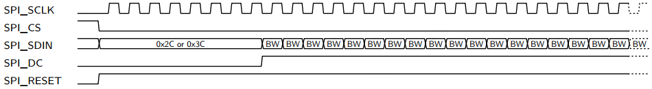
Configuration 0x0E1 (RGB111: Option 4)
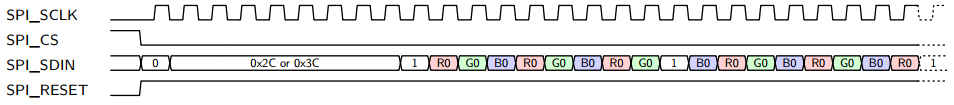
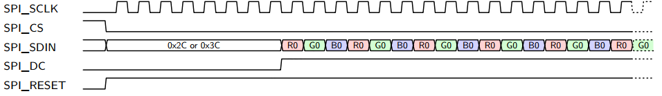
Configuration 0x0C2 (RGB332-Option 0)
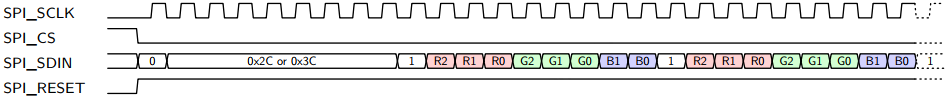
Configuration 0x0C3 (RGB444-Option 0)
Configuration 0x0C5 (RGB565-Option 0)
Configuration 0x0C6 (RGB666-Option 0)

Configuration 0x0C7 (RGB888-Option 0)

DualSPI Output Format
Configuration 0x103 (RGB444-Option 0)
Configuration 0x10B (RGB444-Option 1)
Configuration 0x105 (RGB565-Option 0)
Configuration 0x106 (RGB666-Option 0)
Configuration 0x10E (RGB666-Option 1)
Configuration 0x107 (RGB888-Option 0)
Configuration 0x10F (RGB888-Option 1)
QuadSPI Serial Interface
The QuadSPI serial interface uses SPI_CS (chip enable), SPI_SCLK (serial clock), as well as SPI_SD, SPI_SD1, SPI_SD2, and SPI_SD3 (serial data outputs). The header and the command type are always transmitted through the SPI_SD line, and the data is routed through the SPI_SD, SPI_SD1, SPI_SD2, and SPI_SD3 lines. The header consists of 8 bits. The command word consists of 24 bits, and the data word consists of n bits according to the chosen format.
Configuration 0x143 (RGB444-Option 0)
Configuration 0x145 (RGB565-Option 0)
Configuration 0x146 (RGB666-Option 0)
Configuration 0x147 (RGB888-Option 0)
Registers
MODE
- Name: Mode Register
- Description: General control register that activates the DC controller and various parameters, sets the timing signals’ polarity, and chooses the output display formats to meet LCD color specifications.
- Base Address: 0x4002C000
- Offset: 0x000
- Reset Value: 0x00000000
| Bits | Field Name | RW | Reset | Description |
|---|---|---|---|---|
31 |
EN |
R |
0x0 |
When set to 1, the DC controller is activated. |
30:18 |
RSVD |
R |
Reserved bits |
|
17 |
SINGLE_FRAME |
RW |
0x0 |
When set to 1, single frame update is enabled. |
16:10 |
RSVD |
R |
Reserved bits |
|
9 |
FORMAT |
RW |
0x0 |
Selects a format.
|
8:1 |
RSVD |
R |
Reserved bits |
|
0 |
TEST_MODE |
RW |
0x0 |
Test mode
|
CLK_DIV
- Name: Clock Divider Register
- Description: Set proper timing with divisor control bits and specify the number of lines to be prefetched before the start of frame.
- Base Address: 0x4002C000
- Offset: 0x004
- Reset Value: 0x00000401
| Bits | Field Name | RW | Reset | Description |
|---|---|---|---|---|
31:27 |
OPTIONAL_DIV |
RW |
0x00 |
Value of optional clock divider
|
26:6 |
RSVD |
R |
Reserved bits |
|
0:5 |
PRIMARY_DIV |
RW |
0x00 |
Value of primary clock divider
|
BG_COLOR
- Name: Background Color Register
- Description: This register specifies the main background color.
- Base Address: 0x4002C000
- Offset: 0x008
- Reset Value: 0x00000000
| Bits | Field Name | RW | Reset | Description |
|---|---|---|---|---|
31:24 |
COLOR_BLUE |
RW |
0x0 |
Color red is used as background color. |
23:16 |
COLOR_GREEN |
RW |
0x0 |
Color green is used as background color. |
15:8 |
COLOR_BLUE |
RW |
0x0 |
Color blue is used as background color. |
0:7 |
COLOR_ALPHA |
RW |
0x0 |
Color alpha is used as background color. |
RES
- Name: X and Y Resolutions Register
- Description: This register specifies the main X and Y resolutions.
- Base Address: 0x4002C000
- Offset: 0x00C
- Reset Value: 0x00000000
| Bits | Field Name | RW | Reset | Description |
|---|---|---|---|---|
31:16 |
X_RES |
RW |
0x0 |
Value of X resolution in pixels |
15:0 |
Y_RES |
RW |
0x0 |
Value of Y resolution in pixels |
PLAY
- Name: Play Register
- Description: Write any value to this register at the end of the programming sequence to trigger the display controller.
- Base Address: 0x4002C000
- Offset: 0x010
- Reset Value: 0x00000000
| Bits | Field Name | RW | Reset | Description |
|---|---|---|---|---|
31:0 |
VALUE |
RW |
0x0 |
Trigger the frame generation process. |
INTERFACE_CFG
- Name: Interface Configuration Register
- Description: The activation of SPI 3-/4-wire interfaces
- Base Address: 0x4002C000
- Offset: 0x028
- Reset Value: 0x00000000
| Bits | Field Name | RW | Reset | Description |
|---|---|---|---|---|
31 |
INTERFACE_EN |
RW |
0x0 |
When set to 1, the SPI interfaces are activated. |
30 |
SW_CS_EN |
RW |
0x0 |
When set to 1, the value of the CSX signal of the SPI interfaces can be configured from the INTERFACE_CFG[29] register bit. |
29 |
CS_VAL |
RW |
0x0 |
Sets the value of SPI_CS signal:
|
28:27 |
RSVD |
R |
Reserved bits |
|
26 |
CLEAR_FIFO |
RW |
0x0 |
When set to 1, it clears the data FIFO and the command FIFO of the SPI interfaces. |
25 |
RSVD |
R |
Reserved bit |
|
24 |
INVERT_PIXEL_ORDER |
RW |
0x0 |
Invert pixel order. |
23-22 |
SPI3/4_EN |
RW |
0x0 |
Set the SPI 3-wire or 4-wire mode:
|
21 |
BACK_PRESSURE |
RW |
0x0 |
When set to 1, back-pressure for SPI interfaces is enabled. |
20 |
CLK_PHASE |
RW |
0x0 |
Sets SPI clock phase. |
19 |
CLK_POLARITY |
RW |
0x0 |
Sets SPI clock polarity. |
18:12 |
RSVD |
R |
Reserved bits |
|
11 |
DUALSPI_SUB_PIXEL |
RW |
0x0 |
When set to 1, DualSPI sub-pixel transaction is enabled. |
10:9 |
MODE |
RW |
0x0 |
Set mode of operation- SPI/DualSPI/QuadSPI/QuadSPI DDR:
|
8:6 |
INTERFAC |
RW |
0x0 |
The serial interface(SPI) mode:
|
3:5 |
DATA_ORDER |
RW |
0x0 |
Set the data order of the 8-bit data word:
|
2:0 |
COLOR_FORMAT |
RW |
0x0 |
Set the color format for DBI Type-B/SPI interfaces:
|
LAYER0_MODE
- Name: Layer 0 Mode Register
- Description: Activate and set-up layer 0.
- Base Address: 0x4002C000
- Offset: 0x030
- Reset Value: 0x00000000
| Bits | Field Name | RW | Reset | Description |
|---|---|---|---|---|
31 |
LAYER0_EN |
RW |
0x0 |
When set to 1, layer n is enabled. |
30 |
FORCE_GLOBAL_ALPHA |
RW |
0x0 |
When set to 1, force alpha with global alpha. |
29:24 |
RSVD |
R |
Reserved bits |
|
23:16 |
GLOBAL_ALPHA |
RW |
0x0 |
Alpha layer global value (range: 0x00-0xFF) |
15:12 |
DST_BLEND |
RW |
0x0 |
Destination blending function for layer 0
|
11:8 |
SRC_BLEND |
RW |
0x0 |
Source blending function for layer 0.
|
7:6 |
RSVD |
R |
Reserved bits |
|
5 |
REG_PROTECTION |
RW |
0x0 |
Enable register protection for DC layer registers. When register protection is enabled, the layer registers take effect in the design only when frame end occurs. Register reading functionality from register file remains the same. |
4:0 |
LAYER0_COLOR_MODE |
RW |
0x0 |
Color mode for layer 0.
|
LAYER0_START
- Name: Layer 0 Start Register
- Description: X and Y start dimensions of layer 0
- Base Address: 0x4002C000
- Offset: 0x034
- Reset Value: 0x00000000
| Bits | Field Name | RW | Reset | Description |
|---|---|---|---|---|
31:16 |
LAYER0_X_POSITION |
RW |
0x0 |
Specify the pixel offset of the starting X dimension of layer 0. |
15:0 |
LAYER0_Y_POSITION |
RW |
0x0 |
Specify the pixel offset of the starting Y dimension of layer 0. |
LAYER0_SIZE
- Name: Layer 0 Size Register
- Description: X and Y size of layer 0
- Base Address: 0x4002C000
- Offset: 0x038
- Reset Value: 0x00000000
| Bits | Field Name | RW | Reset | Description |
|---|---|---|---|---|
31:16 |
LAYER0_X_SIZE |
RW |
0x0 |
Specify the pixel size of the layer 0 in the X dimension. |
15:0 |
LAYER0_Y_SIZE |
RW |
0x0 |
Specify the pixel size of the layer 0 in the Y dimension. |
LAYER0_ADDR
- Name: Layer 0 Address Register
- Description: This register specifies the start address of the framebuffer to be accessed by layer 0.
- Base Address: 0x4002C000
- Offset: 0x03C
- Reset Value: 0x00000000
| Bits | Field Name | RW | Reset | Description |
|---|---|---|---|---|
31:0 |
ADDR |
RW |
0x0 |
Specify the start address of framebuffer for layer 0. |
LAYER0_STRIDE
- Name: Layer 0 Stride Register
- Description: This register specifies the stride and the AXI bus burst of layer 0.
- Base Address: 0x4002C000
- Offset: 0x040
- Reset Value: 0x00000000
| Bits | Field Name | RW | Reset | Description |
|---|---|---|---|---|
31:26 |
RSVD |
R |
Reserved bits |
|
25 |
DMA_PREFETCH_EN |
RW |
0x0 |
DMA prefetch in layer 0
|
24:17 |
RSVD |
R |
Reserved bits |
|
16 |
INCR16_EN |
RW |
0x0 |
When set to 1, INCR16 bursts in layer 0 are allowed. |
15:0 |
Y_POSITION |
RW |
0x0 |
Specify the stride, which is the distance from line to line in bytes for layer 0 memory. |
LAYER0_RES
- Name: Layer 0 Resolution Register
- Description: This register specifies X and Y start dimensions for the resolution of layer 0.
- Base Address: 0x4002C000
- Offset: 0x044
- Reset Value: 0x00000000
| Bits | Field Name | RW | Reset | Description |
|---|---|---|---|---|
31:16 |
X_RESOLUTION |
RW |
0x0 |
Specify the layer 0 pixel resolution in the X dimension. |
15:0 |
Y_RESOLUTION |
RW |
0x0 |
Specify the layer 0 pixel resolution in the Y dimension. |
LAYER1_MODE
- Name: Layer 1 Mode Register
- Description: Activate and set-up layer 1.
- Base Address: 0x4002C000
- Offset: 0x050
- Reset Value: 0x00000000
| Bits | Field Name | RW | Reset | Description |
|---|---|---|---|---|
31 |
LAYER1_EN |
RW |
0x0 |
When set to 1, layer n is enabled. |
30 |
FORCE_GLOBAL_ALPHA |
RW |
0x0 |
When set to 1, force alpha with global alpha. |
29:24 |
RSVD |
R |
Reserved bits |
|
23:16 |
GLOBAL_ALPHA |
RW |
0x0 |
Alpha layer global value (range: 0x00-0xFF) |
15:12 |
DST_BLEND |
RW |
0x0 |
Destination blending function for layer 1.
|
11:8 |
SRC_BLEND |
RW |
0x0 |
Source blending function for layer 1.
|
7:6 |
RSVD |
R |
Reserved bits |
|
5 |
REG_PROTECTION |
RW |
0x0 |
Enable register protection for DC layer registers. When register protection is enabled, the layer registers take effect in the design only when frame end occurs. Register reading functionality from register file remains the same. |
4:0 |
LAYER1_COLOR_MODE |
RW |
0x0 |
Color mode for layer 1.
|
LAYER1_START
- Name: Layer 1 Start Register
- Description: X and Y start dimensions of layer 1
- Base Address: 0x4002C000
- Offset: 0x054
- Reset Value: 0x00000000
| Bits | Field Name | RW | Reset | Description |
|---|---|---|---|---|
31:16 |
LAYER1_X_POSITION |
RW |
0x0 |
Specify the pixel offset of the starting X dimension of layer 1. |
15:0 |
LAYER1_Y_POSITION |
RW |
0x0 |
Specify the pixel offset of the starting Y dimension of layer 1. |
LAYER1_SIZE
- Name: Layer 1 Size Register
- Description: X and Y size of layer 1
- Base Address: 0x4002C000
- Offset: 0x058
- Reset Value: 0x00000000
| Bits | Field Name | RW | Reset | Description |
|---|---|---|---|---|
31:16 |
LAYER1_X_SIZE |
RW |
0x0 |
Specify the pixel size of the layer 1 in the X dimension. |
15:0 |
LAYER1_Y_SIZE |
RW |
0x0 |
Specify the pixel size of the layer 1 in the Y dimension. |
LAYER1_ADDR
- Name: Layer 1 Address Register
- Description: This register specifies the start address of the framebuffer to be accessed by layer 1.
- Base Address: 0x4002C000
- Offset: 0x05C
- Reset Value: 0x00000000
| Bits | Field Name | RW | Reset | Description |
|---|---|---|---|---|
31:0 |
ADDR |
RW |
0x0 |
Specify the start address of framebuffer for layer 1. |
LAYER1_STRIDE
- Name: Layer 1 Stride Register
- Description: This register specifies the stride and the AXI bus burst of layer 1.
- Base Address: 0x4002C000
- Offset: 0x060
- Reset Value: 0x00000000
| Bits | Field Name | RW | Reset | Description |
|---|---|---|---|---|
31:26 |
RSVD |
R |
Reserved bits |
|
25 |
DMA_PREFETCH_EN |
RW |
0x0 |
DMA prefetch in layer 1
|
24:17 |
RSVD |
R |
Reserved bits |
|
16 |
INCR16_EN |
RW |
0x0 |
When set to 1, INCR16 bursts in layer 1 are allowed. |
15:0 |
Y_POSITION |
RW |
0x0 |
Specify the stride, which is the distance from line to line in bytes for layer 1 memory. |
LAYER1_RES
- Name: Layer 1 Resolution Register
- Description: This register specifies X and Y start dimensions for the resolution of layer 1.
- Base Address: 0x4002C000
- Offset: 0x064
- Reset Value: 0x00000000
| Bits | Field Name | RW | Reset | Description |
|---|---|---|---|---|
31:16 |
X_RESOLUTION |
RW |
0x0 |
Specify the layer 1 pixel resolution in the X dimension. |
15:0 |
Y_RESOLUTION |
RW |
0x0 |
Specify the layer 1 pixel resolution in the Y dimension. |
INTERFACE_CMD
- Name: Interface Command Register
- Description: Command register to read/write commands from/to SPI interfaces
- Base Address: 0x4002C000
- Offset: 0x0E8
- Reset Value: 0x00000000
| Bits | Field Name | RW | Reset | Description |
|---|---|---|---|---|
31 |
BASE_ADDR_FLAG |
RW |
0x0 |
Being set to 0 indicates that the command data is the base address for partial update. Applied on SPI type. |
30 |
SEND_DATA |
RW |
0x0 |
Send direct data of type command to the SPI interfaces. |
29:28 |
CMD_WIDTH |
RW |
0x0 |
Determine the command width. Applicable only to QuadSPI.
|
27 |
QSPI_SERIAL_EN |
RW |
0x0 |
Being set to 1 means switching to serial transmission of the command. Applicable only to QuadSPI. |
26 |
READ_EN |
RW |
0x0 |
When set to 1, read mode is enabled. |
25 |
RSVD |
R |
Reserved bit |
|
24 |
CMD_LINE_EN |
RW |
0x0 |
When set to 1, store internally a command type which is transmitted at the beginning of each scanline. |
23:16 |
RSVD |
R |
Reserved bits |
|
15:0 |
DATA |
RW |
0x0 |
Data to be sent to the SPI interfaces |
INTERFACE_RDAT
- Name: Interface Read Data Register
- Description: Data read by DBI Type-B/SPI interfaces is stored in the register.
- Base Address: 0x4002C000
- Offset: 0x0EC
- Reset Value: 0x00000000
| Bits | Field Name | RW | Reset | Description |
|---|---|---|---|---|
31:30 |
READ_CYCLES |
RW |
0x0 |
On write: Specify the number of read cycles.
On read: Read data from DBI Type-B/SPI interfaces (high bits). |
29:0 |
READ_DATA |
R |
0x0 |
Read data from DBI Type-B/SPI interfaces (low bits). |
CFG
- Name: Configuration Register
- Description: Information register of the layers activation and setup. The reset value of this register changes according to the selected configuration.
- Base Address: 0x4002C000
- Offset: 0x0F0
- Reset Value: 0x01003130
| Bits | Field Name | RW | Reset | Description |
|---|---|---|---|---|
31 |
LAYER3_YUV_MEM_EN |
R |
0x0 |
Indicates that layer 3 has YUV Memory. |
30 |
LAYER2_YUV_MEM_EN |
R |
0x0 |
Indicates that layer 2 has YUV Memory. |
29 |
LAYER1_YUV_MEM_EN |
R |
0x0 |
Indicates that layer 1 has YUV Memory. |
28 |
LAYER0_YUV_MEM_EN |
R |
0x0 |
Indicates that layer 0 has YUV Memory. |
27:25 |
RSVD |
R |
Reserved bits |
|
24 |
SPI_EN |
R |
0x1 |
Indicates that SPI interface is enabled. |
23 |
LAYER3_GAMMA_EN |
R |
0x0 |
Indicates that layer 3 has Gamma LUT. |
22 |
RSVD |
R |
Reserved bit |
|
21 |
LAYER3_BLENDER_EN |
R |
0x0 |
Indicates that layer 3 has blender. |
20 |
LAYER3_EN |
R |
0x0 |
Indicates that layer 3 is enabled. |
19 |
LAYER2_GAMMA_EN |
R |
0x0 |
Indicates that layer 2 has Gamma LUT. |
18 |
RSVD |
R |
Reserved bit |
|
17 |
LAYER2_BLENDER_EN |
R |
0x0 |
Indicates that layer 2 has blender. |
16 |
LAYER2_EN |
R |
0x0 |
Indicates that layer 2 is enabled. |
15 |
LAYER1_GAMMA_EN |
R |
0x0 |
Indicates that layer 1 has Gamma LUT. |
14 |
RSVD |
R |
Reserved bit |
|
13 |
LAYER1_BLENDER_EN |
R |
0x1 |
Indicates that layer 1 has blender. |
12 |
LAYER1_EN |
R |
0x1 |
Indicates that layer 1 is enabled. |
11 |
LAYER0_GAMMA_EN |
R |
0x0 |
Indicates that layer 0 has Gamma LUT. |
10 |
RSVD |
R |
Reserved bit |
|
9 |
LAYER0_BLENDER_EN |
R |
0x0 |
Indicates that layer 0 has blender. |
8 |
LAYER0_EN |
R |
0x1 |
Indicates that layer 0 is enabled. |
7 |
RGB_TO_YUV_EN |
R |
0x0 |
Indicates that RGB to YUV/YCbCr converter is enabled. |
6 |
DBI_TYPEB_EN |
R |
0x0 |
Indicates that DBI Type-B interface is enabled. |
5 |
YUV_CONVERTER_EN |
R |
0x1 |
Indicates that high quality YUV/YCbCr converter is enabled. |
4 |
FORMAT_EN |
R |
0x1 |
Indicates that formatting is enabled. |
3 |
DITHER_EN |
R |
0x0 |
Indicates that dithering is enabled. |
2 |
RSVD |
R |
Reserved bit |
|
1 |
CURSOR_EN |
R |
0x0 |
Indicates that cursor is enabled. |
0 |
GAMMA_PALETTE_EN |
R |
0x0 |
Indicates that Global Gamma/Palette is enabled. |
ID
- Name: Identification Register
- Description: This register specifies the identification of the DC.
- Base Address: 0x4002C000
- Offset: 0x0F4
- Reset Value: 0x87452365
| Bits | Field Name | RW | Reset | Description |
|---|---|---|---|---|
31:0 |
ID |
R |
0x87452365 |
Constant ID value |
INT
- Name: Interrupt Register
- Description: This register specifies the interrupt of DC.
- Base Address: 0x4002C000
- Offset: 0x0F8
- Reset Value: 0x00000001
| Bits | Field Name | RW | Reset | Description |
|---|---|---|---|---|
31 |
IRQ_TRIGGER |
R |
0x0 |
Interrupt request trigger control
|
30 |
IRQ_UNDERWAY |
R |
0x0 |
Indicates IRQ is underway. |
29:7 |
RSVD |
R |
Reserved bits |
|
6 |
CMD_INT_EN |
RW |
0x0 |
When set to 1, signal an interrupt when SPI/DBI interfaces have finished the transmission of the commands. |
5 |
FRAME_CPLT_INT_EN |
RW |
0x0 |
When set to 1, signal an interrupt when SPI/DBI interfaces have finished the transmission of the frame. |
4 |
FRMAE_END_INT_EN |
RW |
0x0 |
When set to 1, signal an interrupt on frame end. |
3 |
TE_INT_EN |
RW |
0x0 |
When set to 1, TE interrupt is enabled. |
2 |
RSVD |
R |
Reserved bit |
|
1 |
HSYNC_INT_EN |
RW |
0x0 |
When set to 1, HSYNC interrupt is enabled. |
0 |
VSYNC_INT_EN |
RW |
0x1 |
When set to 1, VSYNC interrupt is enabled. |
STAT
- Name: Status Register
- Description: This register specifies the status of DC.
- Base Address: 0x4002C000
- Offset: 0x0FC
- Reset Value: 0x00000000
| Bits | Field Name | RW | Reset | Description |
|---|---|---|---|---|
31:19 |
RSVD |
R |
Reserved bits |
|
18 |
GPI_STACK |
R |
0x0 |
Indicates GPI gets stack during packet transaction. |
17 |
CRC_READY |
R |
0x0 |
Indicates CRC register read is ready. |
16 |
SPI_RW |
R |
0x0 |
Indicates read/write operation on SPI. |
15 |
FIFO_ACK |
R |
0x0 |
Indicates the DBI/SPI command FIFO ACK. |
14 |
CS_STATUS |
R |
0x0 |
Indicates DBI/SPI CS status. |
13 |
FRAME_END |
R |
0x0 |
Indicates frame ends. |
12 |
SPI_PENDING |
R |
0x0 |
Indicates pending output transaction in DBI Type-B/SPI interfaces. |
11 |
CMD_PENDING |
R |
0x0 |
Indicates pending commands in DBI Type-B/SPI interfaces. |
10 |
DATA_PENDING |
R |
0x0 |
Indicates pending RGB data in DBI Type-B/SPI interfaces. |
9 |
RSVD |
R |
Reserved bit |
|
8 |
TEARING_EFFECT |
R |
0x0 |
Indicates DBI Type-B/SPI tearing effect. |
7 |
STICKY_UNDERFLOW |
R |
0x0 |
Indicates sticky underflow. This bit is cleared when interrupt register is written. |
6 |
CUR_UNDERFLOW |
R |
0x0 |
Indicates current underflow. |
5 |
LAST_LOW |
R |
0x0 |
Indicates that the last row is currently displayed. |
4 |
CSYNC_STAT |
R |
0x0 |
Indicates the CSYNC signal status (0 or 1) at the current time of reading. |
3 |
VSYNC_STAT |
R |
0x0 |
Indicates the VSYNC signal status and the tearing effect signal status (0 or 1) at the current time of reading. |
2 |
HSYNC_STAT |
R |
0x0 |
Indicates the HSYNC signal status (0 or 1) at the current time of reading. |
1 |
DE_STAT |
R |
0x0 |
Indicates the DE signal status (0 or 1) at the current time of reading. |
0 |
DC_STAT |
R |
0x0 |
Indicates that the controller is not in active vertical blanking. |
COLOR_MODE
- Name: Color Mode Register
- Description: This register specifies the color mode of DC.
- Base Address: 0x4002C000
- Offset: 0x100
- Reset Value: 0x0067FF59
| Bits | Field Name | RW | Reset | Description |
|---|---|---|---|---|
31:29 |
RSVD |
R |
Reserved bits |
|
28:23 |
RSVD |
R |
Reserved bits |
|
22 |
ARGB4444 |
R |
0x1 |
Setting to zero indicates that the ARGB4444 16-bit color format is disabled. |
21 |
RGBA4444 |
R |
0x1 |
Setting to zero indicates that the RGBA4444 16-bit color format is disabled. |
20:19 |
RSVD |
R |
Reserved bits |
|
18 |
TSC6 |
R |
0x1 |
High value indicates that TSC6 is disabled. |
17 |
TSC4 |
R |
0x1 |
High value indicates that TSC4 is disabled. |
16 |
LUT8 |
R |
0x1 |
Setting to zero indicates that the LUT8 color format is disabled. |
15 |
RGBA5551 |
R |
0x1 |
Setting to zero indicates that the RGBA5551 16-bit color format is disabled. |
14 |
ABGR8888 |
R |
0x1 |
Setting to zero indicates that the ABGR8888 32-bit color format is disabled. |
13 |
RGB332 |
R |
0x1 |
Setting to zero indicates that the RGB332 8-bit color format is disabled. |
12 |
RGB565 |
R |
0x1 |
Setting to zero indicates that the RGB565 16-bit color format is disabled. |
11 |
ARGB8888 |
R |
0x1 |
Setting to zero indicates that the ARGB8888 32-bit color format is disabled. |
10 |
L8 |
R |
0x1 |
Setting to zero indicates that the L8 color format is disabled. |
9 |
L1 |
R |
0x1 |
Setting to zero indicates that the L1 color format is disabled. |
8 |
L4 |
R |
0x1 |
Setting to zero indicates that the L4 color format is disabled. |
7 |
YUYV |
R |
0x0 |
Setting to zero indicates that the YUYV color format is disabled. |
6 |
RGB888 |
R |
0x1 |
Setting to zero indicates that the RGB888 24-bit color format is disabled. |
5 |
YUY2 |
R |
0x0 |
Setting to zero indicates that the YUY2 color format is disabled. |
4 |
RGBA8888 |
R |
0x1 |
Setting to zero indicates that the RGBA8888 32-bit color format is disabled. |
3 |
BGRA8888 |
R |
0x1 |
Setting to zero indicates that the BGRA8888 32-bit color format is disabled. |
2 |
V_YUV420 |
R |
0x0 |
Setting to zero indicates that the V_YUV420 color format is disabled. |
1 |
TLYUV420 |
R |
0x0 |
Setting to zero indicates that the TLYUV420 color format is disabled. |
0 |
TSC4_TSC6 |
R |
0x1 |
Setting to zero indicates that the TSC4/TSC6 proprietary color format is disabled. |
CRC
- Name: CRC Check Register
- Description: This register specifies the CRC value.
- Base Address: 0x4002C000
- Offset: 0x184
- Reset Value: 0x00000000
| Bits | Field Name | RW | Reset | Description |
|---|---|---|---|---|
31:0 |
CRC |
R |
0x0 |
CRC value if CRC error exists |
CLK_CTRL
- Name: Clock Control Register
- Description: Controls the clock gaters and the routing of format and pixel clock.
- Base Address: 0x4002C000
- Offset: 0x1A8
- Reset Value: 0x00000000
| Bits | Field Name | RW | Reset | Description |
|---|---|---|---|---|
31:28 |
RSVD |
R |
Reserved bits |
|
27 |
LAYER1_BUS_CLK_BYPASS |
RW |
0x0 |
Layer 1 bus clock clock-gater bypass |
26 |
LAYER1_PIXEL_CLK_BYPASS |
RW |
0x0 |
Layer 1 pixel clock clock-gater bypass |
25 |
LAYER0_BUS_CLK_BYPASS |
RW |
0x0 |
Layer 0 bus clock clock-gater bypass |
24 |
LAYER0_PIXEL_CLK_BYPASS |
RW |
0x0 |
Layer 0 pixel clock clock-gater bypass |
23 |
REGFILE_BYPASS |
RW |
0x0 |
RegFile clock-gaters bypass |
22 |
BYPASS |
RW |
0x0 |
Clock-gaters bypass |
21:3 |
RSVD |
R |
Reserved bits |
|
2 |
CLK_SWAP |
RW |
0x0 |
Pixel generation and format clock swap |
1 |
CLK_POLARITY |
RW |
0x0 |
Invert (output) clock polarity. |
0 |
CLK_DIV_EN |
RW |
0x0 |
Enable clock divider. |
FORMAT_CTRL
- Name: CS Format Control Register
- Description: Control CS format.
- Base Address: 0x4002C000
- Offset: 0x1AC
- Reset Value: 0x00000000
| Bits | Field Name | RW | Reset | Description |
|---|---|---|---|---|
31:16 |
RSVD |
R |
Reserved bits |
|
15:13 |
CS_END_DELAY |
RW |
0x0 |
Set the delay that begins at the last negative edge of SPI_CLK and ends at the CS deactivation. Values of bits [15:13] while reading from a panel in SDR mode and chip phase is 1:
|
12:10 |
CS_BEGIN_DELAY |
RW |
0x0 |
Set the delay that begins at the CS activation and ends at the first positive edge of SPI_CLK. Values of bits [12:10] in SDR (Single Data Rate) and DDR (Dual Data Rate) modes:
The above equations apply to both write and read modes regardless the values of chip phase and polarity. |
9:0 |
RSVD |
R |
Reserved bits |
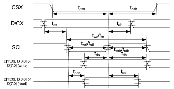
Electrical Specifications
The timing of this the DC module meets the timing standard of MIPI type C, as follows:
| Parameter | Description | Min. | Typ. | Max. | Unit |
|---|---|---|---|---|---|
| fsck | Clock frequency | 48 | M | ||
| tcss | CSX Chip Select setup time(Write) | 4T | ns | ||
| tcsh | CSX Chip Select setup time(Read) | 4T | ns | ||
| tas | D/CX Address setup time | T | ns | ||
| tah | D/CX Address hold time | T | ns | ||
| twc | SCL Write cycle | 10T | ns | ||
| twrh | SCL H duration(Write) | 4T | ns | ||
| twrl | SCL L duration(Write) | 4T | ns | ||
| trc | SCL Read cycle | 15T | ns | ||
| trdh | SCL H duration(Read) | 6T | ns | ||
| trdl | SCL L duration(Read) | 6T | ns | ||
| tds | Write data setup time | 15 | ns | ||
| tdh | Write data hold time | 25 | ns | ||
| tacc | Access time | 10 | ns | ||
| tod | Output disable time | T | ns |
Temperature = -30°C to 70°C; VDDI range: dependent on Logic High level input voltage classification; GND = 0 V; T = 10 (±0.5) ns