SPI
Introduction
GR5526 SoC has two Serial Peripheral Interface (SPI) instances.
- 1 SPI Master (SPIM) with two slave select lines that can interface to up to two slaves that share the same lines with separate selects.
- 1 SPI Slave (SPIS) that can connect to a single master.
Main Features
Main features of the SPIM/SPIS modules include:
- Motorola SPI support
- 2 slave select lines for master mode to support up to 2 slaves.
- Built-in 16 word RX/TX FIFOs for continuous SPI bursts.
- Transfer data size up to 32 bits.
- Programmable output interface frequency up to 48 MHz for SPIM and 16 MHz for SPIS.
- Supports SPI four modes for different clock edge and phase configurations.
- DMA support
- Maskable interrupt generation
Block Diagram
图 37 shows the SPI Controller with the following functions and interfaces:
- APB interface and DMA Controller Interface
- Transmit and receive FIFO controllers and an FSM controller
- Register block
- Shift control and interrupt logic

Functional Description
Motorola Serial Peripheral Interface
With the SPI, the clock polarity (SCPOL) configuration parameter determines whether the inactive state of the serial clock is high or low. To transmit data, both SPI peripherals must have identical serial clock phase (SCPH, control by CTRL0[6]) and clock polarity (SCPOL, control by CTRL0[7]) values. The data frame can be 4 bits to 32 bits.
When the configuration parameter SCPH = 0, data transmission begins on the falling edge of the slave select signal. The first data bit is captured by the master and slave peripherals on the first edge of the serial clock; therefore, valid data must be present on the txd and rxd lines prior to the first serial clock edge.
图 38 shows a timing diagram for a single SPI data transfer with SCPH = 0 (CTRL0[6] = 0). The serial clock is shown for configuration parameters SCPOL = 0 (CTRL0[7] = 0) and SCPOL = 1 (CTRL0[7] = 1).
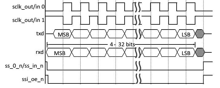
The following signals are illustrated in the timing diagrams in this section:
- sclk_out – serial clock from SPI block master (master configuration only)
- sclk_in – serial clock from SPI block slave (slave configuration only)
- txd – transmit data line for the SPI block master/slave
- rxd – receive data line for the SPI block master/slave
- ss_0_n – slave select signal from SPI block master (master configuration only)
- ss_in_n – slave select input to the SPI block slave
- ss_oe_n – output enable for the SPI block master/slave
Two different modes of continuous data transfers are supported when SCPH = 0; the selection of the desired operation mode is done by configuring bit24 (S_ST_EN) of the CTRL0 register:
- When CTRL0[24] is programmed to 1, SPI block toggles the slave select signal between frames, and the serial clock is held to its default value while the slave select signal is active; this operating mode is illustrated in 图 39.
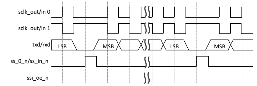
图 39 Serial format continuous transfers (SCPH = 0) when CTRL0[24] = 1 - When CTRL0[24] is programmed to 0, the slave select signal stays low and the serial clock runs continuously for the duration of the transfer; this operating mode is illustrated in 图 40.
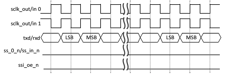
图 40 Serial format continuous transfers (SCPH = 0) when CTRL0[24] = 0
When the configuration parameter SCPH = 1 (CTRL0[6] = 1), both master and slave peripherals begin transmitting data on the first serial clock edge after the slave select line is activated. The first data bit is captured on the second (trailing) serial clock edge. Data is propagated by the master and slave peripherals on the leading edge of the serial clock. During continuous data frame transfers, the slave select line may be held active-low until the last bit of the last frame has been captured.

Transmit and Receive FIFO Buffers
The width of both transmit and receive FIFO buffers is fixed at 32 bits. Data frames that are less than 32 bits must be right-justified when written into the transmit FIFO buffer. The shift control logic automatically right-justifies received data in the receive FIFO buffer.
Each data entry in the FIFO buffers contains a single data frame. It is not possible to store multiple data frames in a single FIFO location; for example, users may not store two 8-bit data frames in a single FIFO location. If an 8-bit data frame is required, the upper 8-bits of the FIFO entry are ignored or unused when the serial shifter transmits the data.
Transmit FIFO
The transmit FIFO is loaded by writing to the SPI Controller data register (DATA). Data is popped from the transmit FIFO by the shift control logic into the transmit shift register. The transmit FIFO generates a FIFO empty interrupt request (ssi_txe_intr) when the number of entries in the FIFO is less than or equal to the FIFO threshold value. The threshold value, set through the programmable transmit FIFO threshold level register (TX_FIFO_TL[2:0]), determines the level of FIFO entries at which an interrupt is generated. The threshold value allows users to provide early indication to the processor that the transmit FIFO is nearly empty. A transmit FIFO overflow interrupt (ssi_txo_intr) is generated if users attempt to write data into an already full transmit FIFO.
Receive FIFO
Data is popped from the receive FIFO by reading the SPI Controller data register (DATA). The receive FIFO is loaded from the receive shift register by the shift control logic. The receive FIFO generates a FIFO-full interrupt request (ssi_rxf_intr) when the number of entries in the FIFO is greater than or equal to the FIFO threshold value plus 1. The threshold value, set through programmable receive FIFO threshold level register (RX_FIFO_TL[2:0]), determines the level of FIFO entries at which an interrupt is generated.
The threshold value allows users to provide early indication to the processor that the receive FIFO is nearly full. A receive FIFO overrun interrupt (ssi_rxo_intr) is generated when the receive shift logic attempts to load data into a completely full receive FIFO. However, this newly received data is lost. A receive FIFO underflow interrupt (ssi_rxu_intr) is generated if users attempt to read from an empty receive FIFO. This alerts the processor that the read data is invalid.
SPI Interrupts
The SPI Controller supports combined and individual interrupt requests, each of which can be masked. The combined interrupt request is the OR’ed result of all other SPI Controller interrupts after masking. The system designer has the choice of routing individual interrupt requests or only the combined interrupt request to the Interrupt Controller. All SPI Controller interrupts are level interrupts that share the same active polarity level; users can configure this polarity level as active-high or active-low.
The SPI Controller interrupts are described as follows:
- Transmit FIFO Empty Interrupt (ssi_txe_intr) – Set when the transmit FIFO is equal to or below its threshold value and requires service to prevent an under-run. The threshold value, set through a software-programmable register, determines the level of transmit FIFO entries at which an interrupt is generated. This interrupt is cleared by hardware when data is written into the transmit FIFO buffer, bringing it over the threshold level.
- Transmit FIFO Overflow Interrupt (ssi_txo_intr) – Set when an APB access attempts to write into the transmit FIFO after it has been completely filled. When set, data written from the APB is discarded. This interrupt remains set until users read the transmit FIFO overflow interrupt clear register (TX_FIFO_OIC[0]).
- Receive FIFO Full Interrupt (ssi_rxf_intr) – Set when the receive FIFO is equal to or above its threshold value plus 1 and requires service to prevent an overflow. The threshold value, set through a software-programmable register, determines the level of receive FIFO entries at which an interrupt is generated. This interrupt is cleared by hardware when data is read from the receive FIFO buffer, bringing it below the threshold level.
- Receive FIFO Overflow Interrupt (ssi_rxo_intr) – Set when the receive logic attempts to place data into the receive FIFO after it has been completely filled. When set, newly received data is discarded. This interrupt remains set until users read the receive FIFO overflow interrupt clear register (RX_FIFO_OIC[0]).
- Receive FIFO Underflow Interrupt (ssi_rxu_intr) – Set when an APB access attempts to read from the receive FIFO when it is empty. When set, zeros are read back from the receive FIFO. This interrupt remains set until users read the receive FIFO underflow interrupt clear register (RX_FIFO_UIC[0]).
Transfer Modes
When transferring data on the serial bus, the SPI Controller operates in the modes discussed in this section. The transfer mode (TMOD) is set by writing to bit8 and bit9 of the SPI control register 0 (CTRL0).
The transfer mode setting does not affect the duplex of the serial transfer.
Transmit and Receive
When CTRL0[9:8] = 0x0, both transmit and receive logics are valid. The data transfer occurs as normal according to the selected frame format (serial protocol). Transmit data is popped from the transmit FIFO and sent through the txd (tx data) line to the target device, which replies with data on the rxd (rx data) line. The receive data from the target device is moved from the receive shift register into the receive FIFO at the end of each data frame.
Transmit Only
When CTRL0[9:8] = 0x1, the receive data is invalid and should not be stored in the receive FIFO. The data transfer occurs as normal, according to the selected frame format (serial protocol). Transmit data is popped from the transmit FIFO and sent through the txd line to the target device, which replies with data on the rxd line. At the end of the data frame, the receive shift register does not load its newly received data into the receive FIFO. The data in the receive shift register is overwritten by the next transfer. Users should mask interrupts originating from the receive logic when this mode is entered.
Receive Only
When CTRL0[9:8] = 0x2, the transmit data is invalid. When configured as a slave, the transmit FIFO is never popped in Receive Only mode. The txd output remains at a constant logic level during the transmission. The data transfer occurs as normal according to the selected frame format (serial protocol). The receive data from the target device is moved from the receive shift register into the receive FIFO at the end of each data frame. Users should mask interrupts originating from the transmit logic when this mode is entered.
EEPROM Read
This transfer mode is only valid for master configurations.
When CTRL0[9:8] = 0x3, the transmit data is used to transmit an opcode and/or an address to the EEPROM device. Typically, this takes three data frames (8-bit opcode followed by 8-bit upper address and 8-bit lower address). During the transmission of the opcode and address, no data is captured by the receive logic (as long as the SPI Controller master is transmitting data on its txd line, data on the rxd line is ignored). The SPI Controller master continues to transmit data until the transmit FIFO is empty. Therefore, users should only have enough data frames in the transmit FIFO to supply the opcode and address to the EEPROM. If more data frames are in the transmit FIFO than needed, then read data is lost.
When the transmit FIFO becomes empty (all control information has been sent), data on the receive line (rxd) is valid and is stored in the receive FIFO; the txd output is held at a constant logic level. The serial transfer continues until the number of data frames received by the SPI Controller master matches the value of the NDF (Number of Data Frames) field in the SPI Control register 1 (CTRL1[15:0]) plus 1.
SPI Master Operation
Data transfers are started by the serial-master device. When the SPI Controller is enabled (SPI Enable Register, SSI_EN[0]=1), at least one valid data entry is present in the transmit FIFO and a serial-slave device is selected. When actively transferring data, the busy flag (BUSY) in the status register (STAT[0]) is set. Users must wait until the busy flag is cleared before attempting a new serial transfer.
When the transfer mode is “transmit and receive” or “transmit only” (CTRL0[9:8] = 0x0 or CTRL0[9:8] = 0x1, respectively), transfers are terminated by the shift control logic when the transmit FIFO is empty. For continuous data transfers, users must ensure that the transmit FIFO buffer does not become empty before all the data has been transmitted. The transmit FIFO threshold level (TX_FIFO_TL[2:0]) can be used to early interrupt (ssi_txe_intr) the processor, indicating that the transmit FIFO buffer is nearly empty. When a DMA is used for APB accesses, the DMA transmit data level (DMA_TX_DL[2:0]) can be used to early request (dma_tx_req) the DMA Controller, indicating that the transmit FIFO is nearly empty. The FIFO can then be refilled with data to continue the serial transfer. Users may also write a block of data (at least two FIFO entries) into the transmit FIFO before enabling a serial slave. This ensures that serial transmission does not begin until the number of data frames that make up the continuous transfer are present in the transmit FIFO.
When the transfer mode is “receive only” (CTRL0[9:8] = 0x2), a serial transfer is started by writing one “dummy” data word into the transmit FIFO when a serial slave is selected. The TXD output from the SPI Controller is held at a constant logic level for the duration of the serial transfer. The transmit FIFO is popped only once at the beginning and may remain empty for the duration of the serial transfer. The end of the serial transfer is controlled by the “number of data frames” (NDF) field in control register 1 (CTRL1[15:0]).
If, for example, users want to receive 24 data frames from a serial-slave peripheral, you should program the NDF field with the value 23; the receive logic terminates the serial transfer when the number of frames received is equal to the NDF value + 1. This transfer mode increases the bandwidth of the APB bus as the transmit FIFO never needs to be serviced during the transfer. The receive FIFO buffer should be read each time the receive FIFO generates a FIFO full interrupt request to prevent an overflow.
When the transfer mode is “eeprom_read” (CTRL0[9:8] = 0x3), a serial transfer is started by writing the opcode and/or address into the transmit FIFO when a serial slave (EEPROM) is selected. The opcode and address are transmitted to the EEPROM device, after which read data is received from the EEPROM device and stored in the receive FIFO. The end of the serial transfer is controlled by the NDF field in the control register 1 (CTRL1[15:0]).
The receive FIFO threshold level (RX_FIFO_TL[2:0]) can be used to give early indication that the receive FIFO is nearly full. When a DMA is used for APB accesses, the DMA receive data level (DMA_RX_DL[2:0]) can be used to early request (dma_rx_req) the DMA Controller, indicating that the receive FIFO is nearly full.
SPI Slave Operation
If the SPI Controller slave is receive only (CTRL0[9:8] = 0x2), the transmit FIFO does not need to contain valid data because the data currently in the transmit shift register is resent each time the slave device is selected. The TX_ERR error flag in the status register (STAT[5]) is not set when CTRL0[9:8] = 0x1. Users should mask the transmit FIFO empty interrupt when this mode is used.
If the SPI Controller slave transmits data to the master, users must ensure that data exists in the transmit FIFO before a transfer is initiated by the serial-master device. If the master initiates a transfer to the SPI Controller slave when no data exists in the transmit FIFO, an error flag (TX_ERR) is set in the status register (STAT[5]), and the previously transmitted data frame is resent on txd. For continuous data transfers, users must ensure that the transmit FIFO buffer does not become empty before all the data has been transmitted. The transmit FIFO threshold level register (TX_FIFO_TL[2:0]) can be used to early interrupt (ssi_txe_intr) the processor, indicating that the transmit FIFO buffer is nearly empty. When a DMA Controller is used for APB accesses, the DMA transmit data level register (DMA_TX_DL[2:0]) can be used to early request (dma_tx_req) the DMA Controller, indicating that the transmit FIFO is nearly empty. The FIFO can then be refilled with data to continue the serial transfer. The receive FIFO buffer should be read each time the receive FIFO generates a FIFO full interrupt request to prevent an overflow. The receive FIFO threshold level register (RX_FIFO_TL[2:0]) can be used to give early indication that the receive FIFO is nearly full. When a DMA Controller is used for APB accesses, the DMA receive data level register (DMA_RX_DL[2:0]) can be used to early request (dma_rx_req) the DMA controller, indicating that the receive FIFO is nearly full.
Registers
CTRL0
- Name: SPI Control Register 0
- Description: This register controls the serial data transfer. It is impossible to write to this register when the SPI is enabled.
- Base Address: 0x4000C000 + x*0x100 (x: 0 for master, 1 for slave)
- Offset: 0x00
- Reset Value: 0x01070000
| Bits | Field Name | RW | Reset | Description |
|---|---|---|---|---|
31:25 |
RSVD |
R |
Reserved bits. |
|
24 |
S_ST_EN |
RW |
0x1 |
Slave Select Toggle Enable. When operating in SPI mode with clock phase (SCPH) set to 0, this register controls the behavior of the slave select line (CS) between data frames. If this register field is set to 1 the CS line will toggle between consecutive data frames, with the serial clock (sclk) being held to its default value while CS is high; if this register field is set to 0 the CS will stay low and sclk will run continuously for the duration of the transfer. Note: When the SPI is configured as a slave, this register serves no purpose. |
23:21 |
RSVD |
R |
Reserved bits. |
|
20:16 |
DATA_FRAME_SIZE |
RW |
0x7 |
Data Frame Size in 32-bit transfer size mode. Used to select the data frame size in 32-bit transfer mode. When the data frame size is programmed to be less than 32 bits, the receive data is automatically right-justified by the receive logic, with the upper bits of the receive FIFO zero-padded. You are responsible for making sure that transmit data is right-justified before writing into the transmit FIFO. The transmit logic ignores the upper unused bits when transmitting the data. Value:
|
15:12 |
CTRL_FRAME_SIZE |
RW |
0x0 |
Control Frame Size. Selects the length of the control word for the Microwire frame format. Value:
|
11 |
SHIFT_REG_LOOP |
RW |
0x0 |
Shift Register Loop. Used for testing purposes only. When internally active, connects the transmit shift register output to the receive shift register input. Value:
|
10 |
S_OUT_EN |
RW |
0x0 |
Slave Output Enable. Relevant only when the SPI is configured as a serial-slave device. When configured as a serial master, this bit field has no functionality. Value:
Note: When the SPI is configured as a master, this register serves no purpose. |
9:8 |
XFE_MODE |
RW |
0x0 |
Transfer Mode. Selects the mode of transfer for serial communication. This field does not affect transfer duplicity, and only indicates whether the received or transmitted data is valid.
|
7 |
SERIAL_CLK_POL |
RW |
0x0 |
Serial Clock Polarity. Valid when the frame format (FRF) is set to Motorola SPI. Used to select the polarity of the inactive serial clock, which is held inactive when the SPI master is not actively transferring data on the serial bus. Value:
|
6 |
SERIAL_CLK_PHASE |
RW |
0x0 |
Serial Clock Phase. Valid when the frame format (FRF) is set to Motorola SPI. The serial clock phase selects the relationship of the serial clock with the slave select signal. When SCPH = 0, data is captured on the first edge of the serial clock. When SCPH = 1, the serial clock starts toggling one cycle after the slave select line is activated, and data is captured on the second edge of the serial clock. Value:
|
5:4 |
FRAME_FORMAT |
RW |
0x0 |
Frame Format. Selects which serial protocol transfers the data. Value:
|
3:0 |
RSVD |
R |
Reserved bits. |
CTRL1
- Name: SPI Control Register 1
- Description: This register exists only when the SPI is configured as a master device. Control register 1 controls the end of serial transfers in receive-only mode. It is impossible to write to this register when the SPI is enabled.
- Base Address: 0x4000C000 + x*0x100 (x: 0 for master, 1 for slave)
- Offset: 0x04
- Reset Value: 0x00000000
| Bits | Field Name | RW | Reset | Description |
|---|---|---|---|---|
31:16 |
RSVD |
R |
Reserved bits. |
|
15:0 |
NUM_DATA_FRAME |
RW |
0x0 |
Number of Data Frames. When CTRL0[9:8] = 0x2 or CTRL0[9:8] = 0x3, this register field sets the number of data frames to be continuously received by the SPI. The SPI continues to receive serial data until the number of data frames received is equal to this register value plus 1, which enables you to receive up to 64KB of data in a continuous transfer. Note: When the SPI is configured as a slave, this register serves no purpose. |
SSI_EN
- Name: SPI Enable Register
- Description: This register enables and disables the SPI.
- Base Address: 0x4000C000 + x*0x100 (x: 0 for master, 1 for slave)
- Offset: 0x08
- Reset Value: 0x00000000
| Bits | Field Name | RW | Reset | Description |
|---|---|---|---|---|
31:1 |
RSVD |
R |
Reserved bits. |
|
0 |
SSI_EN |
RW |
0x0 |
SSI Enable. Enables and disables all SPI operations. When disabled, all serial transfers are halted immediately. Transmit and receive FIFO buffers are cleared when the device is disabled. Value:
|
MW_CTRL
- Name: Microwire Control Register
- Description: This register controls the direction of the data word for the half-duplex Microwire serial protocol. It is impossible to write to this register when the SPI is enabled.
- Base Address: 0x4000C000 + x*0x100 (x: 0 for master, 1 for slave)
- Offset: 0x0C
- Reset Value: 0x00000000
| Bits | Field Name | RW | Reset | Description |
|---|---|---|---|---|
31:3 |
RSVD |
R |
Reserved bits. |
|
2 |
MW_HSG |
RW |
0x0 |
Microwire Handshaking. Used to enable and disable the busy/ready handshaking interface for the Microwire protocol. When enabled, the SPI checks for a ready status from the target slave, after the transfer of the last data/control bit, before clearing the BUSY status in the STAT register. Value:
Note: When the SPI is configured as a slave, this register serves no purpose. |
1 |
MW_DIR_DW |
RW |
0x0 |
Microwire Control. Defines the direction of the data word when the Microwire serial protocol is used. Value:
|
0 |
MW_XFE_MODE |
RW |
0x0 |
Microwire Transfer Mode. Defines whether the Microwire transfer is sequential or non-sequential. When sequential mode is used, only one control word is needed to transmit or receive a block of data words. When non-sequential mode is used, there must be a control word for each data word that is transmitted or received. Value:
|
S_EN
- Name: Slave Enable Register
- Description: This register exists only when the SPI is configured as a master device. The register enables the individual slave select output lines from the SPI master.
- Base Address: 0x4000C000 + x*0x100 (x: 0 for master, 1 for slave)
- Offset: 0x10
- Reset Value: 0x00000000
| Bits | Field Name | RW | Reset | Description |
|---|---|---|---|---|
31:2 |
RSVD |
R |
Reserved bits. |
|
1:0 |
SEL_EN |
RW |
0x0 |
Slave Select Enable. Each bit in this register corresponds to a slave select line (CSn) from the SPI master. Value:
Note: When the SPI is configured as a slave, this register serves no purpose. |
BAUD
- Name: Baud Rate Register
- Description: This register exists only when the SPI is configured as a master device. The register derives the frequency of the serial clock that regulates the data transfer. It is impossible to write to this register when the SPI is enabled.
- Base Address: 0x4000C000 + x*0x100 (x: 0 for master, 1 for slave)
- Offset: 0x14
- Reset Value: 0x00000000
| Bits | Field Name | RW | Reset | Description |
|---|---|---|---|---|
31:16 |
RSVD |
R |
Reserved bits. |
|
15:0 |
CLK_DIV |
RW |
0x0 |
SPI Clock Divider. The LSB for this field is always set to 0 and is unaffected by a write operation, which ensures an even value is held in this register. If the value is 0, the serial output clock (sclk_out) is disabled. The frequency of the sclk_out is derived from the following equation: Fsclk_out = Fssi_clk/SCKDV Note: When the SPI is configured as a slave, this register serves no purpose. |
TX_FIFO_TL
- Name: Transmit FIFO Threshold Level Register
- Description: This register controls the threshold value for the transmit FIFO memory.
- Base Address: 0x4000C000 + x*0x100 (x: 0 for master, 1 for slave)
- Offset: 0x18
- Reset Value: 0x00000000
| Bits | Field Name | RW | Reset | Description |
|---|---|---|---|---|
31:3 |
RSVD |
R |
Reserved bits. |
|
2:0 |
TX_FIFO_THD |
RW |
0x0 |
Transmit FIFO Threshold. Controls the level of entries at (or below) which the transmit FIFO controller triggers an interrupt. The FIFO depth is configurable in 16 words; this register is sized to the number of address bits needed to access the FIFO. If users attempt to set this value greater than or equal to the depth of the FIFO, this field is not written and retains its current value. When the number of transmit FIFO entries is less than or equal to this value, the transmit FIFO empty interrupt is triggered. |
RX_FIFO_TL
- Name: Receive FIFO Threshold Level
- Description: This register controls the threshold value for the receive FIFO memory.
- Base Address: 0x4000C000 + x*0x100 (x: 0 for master, 1 for slave)
- Offset: 0x1C
- Reset Value: 0x00000000
| Bits | Field Name | RW | Reset | Description |
|---|---|---|---|---|
31:3 |
RSVD |
R |
Reserved bits. |
|
2:0 |
RX_FIFO_THD |
RW |
0x0 |
Receive FIFO Threshold. Controls the level of entries at (or above) which the receive FIFO controller triggers an interrupt. The FIFO depth is configurable in 16 words. This register is sized to the number of address bits needed to access the FIFO. If users attempt to set this value greater than the depth of the FIFO, this field is not written and retains its current value. When the number of receive FIFO entries is greater than or equal to this value + 1, the receive FIFO full interrupt is triggered. |
TX_FIFO_LV
- Name: Transmit FIFO Level Register
- Description: This register contains the number of valid data entries in the transmit FIFO memory.
- Base Address: 0x4000C000 + x*0x100 (x: 0 for master, 1 for slave)
- Offset: 0x20
- Reset Value: 0x00000000
| Bits | Field Name | RW | Reset | Description |
|---|---|---|---|---|
31:4 |
RSVD |
R |
Reserved bits. |
|
3:0 |
TX_FIFO_LV |
R |
0x0 |
Transmit FIFO Level. Contains the number of valid data entries in the transmit FIFO. |
RX_FIFO_LV
- Name: Receive FIFO Level Register
- Description: This register contains the number of valid data entries in the receive FIFO memory. This register can be ready at any time.
- Base Address: 0x4000C000 + x*0x100 (x: 0 for master, 1 for slave)
- Offset: 0x24
- Reset Value: 0x00000000
| Bits | Field Name | RW | Reset | Description |
|---|---|---|---|---|
31:4 |
RSVD |
R |
Reserved bits. |
|
3:0 |
RX_FIFO_LV |
R |
0x0 |
Receive FIFO Level. Contains the number of valid data entries in the receive FIFO. |
STAT
- Name: Status Register
- Description: This is a read-only register used to indicate the current transfer status, FIFO status, and any transmission/reception errors that may have occurred. The status register may be read at any time.
- Base Address: 0x4000C000 + x*0x100 (x: 0 for master, 1 for slave)
- Offset: 0x28
- Reset Value: 0x00000006
| Bits | Field Name | RW | Reset | Description |
|---|---|---|---|---|
31:7 |
RSVD |
R |
Reserved bits. |
|
6 |
DATA_COLN_ERR |
R |
0x0 |
Data Collision Error. This bit will be set if MISO input is asserted by other master, when the SPI master is in the middle of the transfer. This informs the processor that the last data transfer was halted before completion. This bit is cleared when read. Note: When the SPI is configured as a slave, this register serves no purpose. |
5 |
TX_ERR |
R |
0x0 |
Transmission Error. Set if the transmit FIFO is empty when a transfer is started. Data from the previous transmission is resent on the txd line. This bit is cleared when read. Value:
Note: When the SPI is configured as a master, this register serves no purpose. |
4 |
RX_FIFO_FULL |
R |
0x0 |
Receive FIFO Full. When the receive FIFO is completely full, this bit is set. When the receive FIFO contains one or more empty location, this bit is cleared. Value:
|
3 |
RX_FIFO_NE |
R |
0x0 |
Receive FIFO Not Empty. Set when the receive FIFO contains one or more entries and is cleared when the receive FIFO is empty. This bit can be polled by software to completely empty the receive FIFO. Value:
|
2 |
TX_FIFO_EMPTY |
R |
0x1 |
Transmit FIFO Empty. When the transmit FIFO is completely empty, this bit is set. When the transmit FIFO contains one or more valid entries, this bit is cleared. This bit field does not request an interrupt. Value:
|
1 |
TX_FIFO_NF |
R |
0x1 |
Transmit FIFO Not Full. Set when the transmit FIFO contains one or more empty locations, and is cleared when the FIFO is full. Value:
|
0 |
BUSY |
R |
0x0 |
SSI Busy Flag. When set, indicates that a serial transfer is in progress; when cleared indicates that the SPI is idle or disabled. Value:
|
INT_MASK
- Name: Interrupt Mask Register
- Description: This read/write register masks or enables all interrupts generated by the SPI. When the SPI is configured as a slave device, the MSTIM bit field is not present. This changes the reset value from 0x3F for serial-master configurations to 0x1F for serial-slave configurations.
- Base Address: 0x4000C000 + x*0x100 (x: 0 for master, 1 for slave)
- Offset: 0x2C
- Reset Value: master ? 0x0000003F : 0x0000001F
| Bits | Field Name | RW | Reset | Description |
|---|---|---|---|---|
31:6 |
RSVD |
R |
Reserved bits. |
|
5 |
MULTI_M_CIM |
RW |
0x1 |
Multi-Master Contention Interrupt Mask. Value:
Note: When the SPI is configured as a slave, this register serves no purpose. |
4 |
RX_FIFO_FIM |
RW |
0x1 |
Receive FIFO Full Interrupt Mask Value:
|
3 |
RX_FIFO_OIM |
RW |
0x1 |
Receive FIFO Overflow Interrupt Mask Value:
|
2 |
RX_FIFO_UIM |
RW |
0x1 |
Receive FIFO Underflow Interrupt Mask Value:
|
1 |
TX_FIFO_OIM |
RW |
0x1 |
Transmit FIFO Overflow Interrupt Mask Value:
|
0 |
TX_FIFO_EIM |
RW |
0x1 |
Transmit FIFO Empty Interrupt Mask Value:
|
INT_STAT
- Name: Interrupt Status Register
- Description: This register reports the status of the SPI interrupts after they have been enabled.
- Base Address: 0x4000C000 + x*0x100 (x: 0 for master, 1 for slave)
- Offset: 0x30
- Reset Value: 0x00000000
| Bits | Field Name | RW | Reset | Description |
|---|---|---|---|---|
31:6 |
RSVD |
R |
Reserved bits. |
|
5 |
MULTI_M_CIS |
R |
0x0 |
Multi-Master Contention Interrupt Status Value:
|
4 |
RX_FIFO_FIS |
R |
0x0 |
Receive FIFO Full Interrupt Status Value:
|
3 |
RX_FIFO_OIS |
R |
0x0 |
Receive FIFO Overflow Interrupt Status Value:
|
2 |
RX_FIFO_UIS |
R |
0x0 |
Receive FIFO Underflow Interrupt Status Value:
|
1 |
TX_FIFO_OIS |
R |
0x0 |
Transmit FIFO Overflow Interrupt Status Value:
|
0 |
TX_FIFO_EIS |
R |
0x0 |
Transmit FIFO Empty Interrupt Status Value:
|
RAW_INT_STAT
- Name: Raw Interrupt Status Register
- Description: This read-only register reports the status of the SPI interrupts prior to being enabled.
- Base Address: 0x4000C000 + x*0x100 (x: 0 for master, 1 for slave)
- Offset: 0x34
- Reset Value: 0x00000000
| Bits | Field Name | RW | Reset | Description |
|---|---|---|---|---|
31:6 |
RSVD |
R |
Reserved bits. |
|
5 |
MULTI_M_CRIS |
R |
0x0 |
Multi-Master Contention Raw Interrupt Status Value:
|
4 |
RX_FIFO_FRIS |
R |
0x0 |
Receive FIFO Full Raw Interrupt Status Value:
|
3 |
RX_FIFO_ORIS |
R |
0x0 |
Receive FIFO Overflow Raw Interrupt Status Value:
|
2 |
RX_FIFO_URIS |
R |
0x0 |
Receive FIFO Underflow Raw Interrupt Status Value:
|
1 |
TX_FIFO_ORIS |
R |
0x0 |
Transmit FIFO Overflow Raw Interrupt Status Value:
|
0 |
TX_FIFO_ERIS |
R |
0x0 |
Transmit FIFO Empty Raw Interrupt Status Value:
|
TX_FIFO_OIC
- Name: Transmit FIFO Overflow Interrupt Clear Register
- Description: Transmit FIFO Overflow Interrupt Clear Register.
- Base Address: 0x4000C000 + x*0x100 (x: 0 for master, 1 for slave)
- Offset: 0x38
- Reset Value: 0x00000000
| Bits | Field Name | RW | Reset | Description |
|---|---|---|---|---|
31:1 |
RSVD |
R |
Reserved bits. |
|
0 |
TX_FIFO_OIC |
R |
0x0 |
Clear Transmit FIFO Overflow Interrupt. This register reflects the status of the interrupt. A read from this register clears the txo_intr interrupt; writing has no effect. |
RX_FIFO_OIC
- Name: Receive FIFO Overflow Interrupt Clear Register
- Description: Receive FIFO Overflow Interrupt Clear Register.
- Base Address: 0x4000C000 + x*0x100 (x: 0 for master, 1 for slave)
- Offset: 0x3C
- Reset Value: 0x00000000
| Bits | Field Name | RW | Reset | Description |
|---|---|---|---|---|
31:1 |
RSVD |
R |
Reserved bits. |
|
0 |
RX_FIFO_OIC |
R |
0x0 |
Clear Receive FIFO Overflow Interrupt. This register reflects the status of the interrupt. A read from this register clears the rxo_intr interrupt; writing has no effect. |
RX_FIFO_UIC
- Name: Receive FIFO Underflow Interrupt Clear Register
- Description: Receive FIFO Underflow Interrupt Clear Register.
- Base Address: 0x4000C000 + x*0x100 (x: 0 for master, 1 for slave)
- Offset: 0x40
- Reset Value: 0x00000000
| Bits | Field Name | RW | Reset | Description |
|---|---|---|---|---|
31:1 |
RSVD |
R |
Reserved bits. |
|
0 |
RX_FIFO_UIC |
R |
0x0 |
Clear Receive FIFO Underflow Interrupt. This register reflects the status of the interrupt. A read from this register clears the rxu_intr interrupt; writing has no effect. |
MULTI_M_IC
- Name: Multi-Master Interrupt Clear Register
- Description: Multi-Master Interrupt Clear Register.
- Base Address: 0x4000C000 + x*0x100 (x: 0 for master, 1 for slave)
- Offset: 0x44
- Reset Value: 0x00000000
| Bits | Field Name | RW | Reset | Description |
|---|---|---|---|---|
31:1 |
RSVD |
R |
Reserved bits. |
|
0 |
MULTI_M_IC |
R |
0x0 |
Clear Multi-Master Contention Interrupt. This register reflects the status of the interrupt. A read from this register clears the mst_intr interrupt; writing has no effect. |
INT_CLR
- Name: Interrupt Clear Register
- Description: Interrupt Clear Register.
- Base Address: 0x4000C000 + x*0x100 (x: 0 for master, 1 for slave)
- Offset: 0x48
- Reset Value: 0x00000000
| Bits | Field Name | RW | Reset | Description |
|---|---|---|---|---|
31:1 |
RSVD |
R |
Reserved bits. |
|
0 |
INT_CLR |
R |
0x0 |
Clear Interrupts. This register is set if any of the interrupts below are active. A read clears the txo_intr, rxu_intr, rxo_intr, and the mst_intr interrupts. Writing to this register has no effect. |
DMA_CTRL
- Name: DMA Control Register
- Description: The register is used to enable the DMA Controller interface operation.
- Base Address: 0x4000C000 + x*0x100 (x: 0 for master, 1 for slave)
- Offset: 0x4C
- Reset Value: 0x00000000
| Bits | Field Name | RW | Reset | Description |
|---|---|---|---|---|
31:2 |
RSVD |
R |
Reserved bits. |
|
1 |
TX_DMA_EN |
RW |
0x0 |
Transmit DMA Enable. This bit enables/disables the transmit FIFO DMA channel. Value:
|
0 |
RX_DMA_EN |
RW |
0x0 |
Receive DMA Enable. This bit enables/disables the receive FIFO DMA channel Value:
|
DMA_TX_DL
- Name: DMA Transmit Data Level
- Description: This register controls the threshold value for the transmit FIFO memory.
- Base Address: 0x4000C000 + x*0x100 (x: 0 for master, 1 for slave)
- Offset: 0x50
- Reset Value: 0x00000000
| Bits | Field Name | RW | Reset | Description |
|---|---|---|---|---|
31:3 |
RSVD |
R |
Reserved bits. |
|
2:0 |
DMA_TX_DL |
RW |
0x0 |
Transmit Data Level. This bit field controls the level at which a DMA request is made by the transmit logic. It is equal to the watermark level; that is, the dma_tx_req signal is generated when the number of valid data entries in the transmit FIFO is equal to or below this field value, and TX_DMA_EN = 1. |
DMA_RX_DL
- Name: DMA Receive Data Level
- Description: This register controls the threshold value for the receive FIFO memory.
- Base Address: 0x4000C000 + x*0x100 (x: 0 for master, 1 for slave)
- Offset: 0x54
- Reset Value: 0x00000000
| Bits | Field Name | RW | Reset | Description |
|---|---|---|---|---|
31:3 |
RSVD |
R |
Reserved bits |
|
2:0 |
DMA_RX_DL |
RW |
0x0 |
Receive Data Level. This bit field controls the level at which a DMA request is made by the receive logic. The watermark level = DMA_RX_DL+1; that is, dma_rx_req is generated when the number of valid data entries in the receive FIFO is equal to or above this field value + 1, and RX_DMA_EN=1. |
DATA
- Name: Data Register
- Description: The SPI data register is a 32-bit read/write buffer for the transmit/receive FIFOs. When the register is read, data in the receive FIFO buffer is accessed. When it is written to, data is moved into the transmit FIFO buffer; a write can occur only when SSI_EN[0] = 1. FIFOs are reset when SSI_EN[0] = 0
- Base Address: 0x4000C000 + x*0x100 (x: 0 for master, 1 for slave)
- Offset: 0x60
- Reset Value: 0x00000000
| Bits | Field Name | RW | Reset | Description |
|---|---|---|---|---|
31:0 |
DATA |
RW |
0x0 |
Data Register. When writing to this register, you must right-justify the data. Read data is automatically right-justified. |
RX_SMP_DLY
Name: Receive sample delay Register
Description: This register control the number of SCLK cycles that are delayed (from the default sample time) before the actual sample of the rxd input occurs. It is impossible to write to this register when the SPI is enabled.
- Base Address: 0x4000C000 + x*0x100 (x: 0 for master, 1 for slave)
- Offset: 0xF0
- Reset Value: 0x00000000
| Bits | Field Name | RW | Reset | Description |
|---|---|---|---|---|
3:0 |
RX_SMP_DLY |
RW |
0x0 |
Receive sample delay |
Electrical Specifications
SPIM Electrical Specifications
| Parameter | Description | Min. | Typ. | Max. | Unit |
|---|---|---|---|---|---|
| fSCK | Clock frequency | 48 | MHz | ||
| tCSCK | SCK clock period | 20.83 | ns | ||
| tRSCK | SCK rise time, 15 pF loading | tRF,15pF[1] | ns | ||
| tFSCK | SCK fall time, 15 pF loading | tRF,15pF[1] | ns | ||
| tWSCKH | SCK clock high time | 7.625[2] | ns | ||
| tWSCKL | SCK clock low time | 7.625[2] | ns | ||
| tSUMI | Data input setup time (MISO to SCK edge) | 5 | ns | ||
| tHMI | Data input hold time (SCK edge to MISO change) | 5 | ns | ||
| tVMO | Data output valid time (SCK edge to MOSI valid) | 0 | ns | ||
| tHMO | MOSI hold time after CLK edge | 20 | ns |
[1]The SCK rise time and the SCK fall time are obtained with SPIM timing shown in 图 42.
[2]The SCK clock high time and SCK clock low time are calculated by (tCSCK/2)–tRSCK and (tCSCK/2)–tFSCK, respectively.
The SPIM timing diagram is as below:

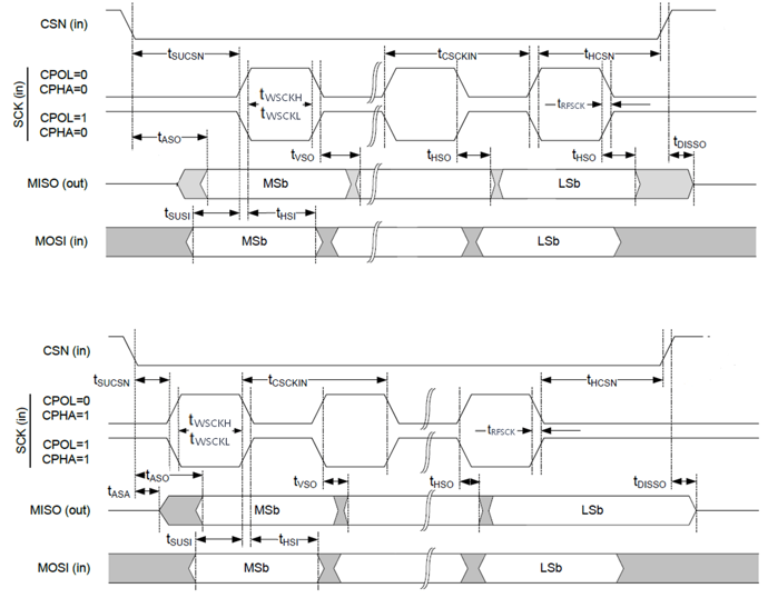
SPIS Electrical Specifications
| Parameter | Description | Min. | Typ. | Max. | Unit |
|---|---|---|---|---|---|
| fSCK | Clock frequency | 16 | MHz | ||
| tCSCK | SCK input clock period | 62.5 | ns | ||
| tRFSCK | SCK input clock rise/fall time | 22 | ns | ||
| tWSCKH | SCK input clock high time | 22 | ns | ||
| tWSCKL | SCK input clock low time | 22 | ns | ||
| tSUCSN | CSN input setup time | 62.5 | ns | ||
| tHCSN | CSN input hold time | 31.25 | ns | ||
| tASO | Data output access time (from CSN to MISO valid) | 62.5 | ns | ||
| tDISSO | Data output disable time (from CSN to MISO disabled) | 62.5 | ns | ||
| tVSO | Data output valid time (from SCK to MISO valid) | 20 | ns | ||
| tHSO | Data output hold time (from SCK to MISO change) | 8 | ns | ||
| tSUSI | Data input setup time (from MOSI to SCK) | 18 | ns | ||
| tHSI | Data input hold time (from SCK to MOSI change) | 0 | ns |
If SPIS performs RX and TX concurrently, the maximum bit rate decreases to 8 Mbps.
The SPIS timing diagram is shown below: