
DSPI
Introduction
DSPI (Display SPI) block implements a display interface that complies with MIPI DBI Type C standard. It is based on SPI protocol and incorporates protocol extensions that are common in the industry. It is important to note that DSPI module is not intended to be used as a general-purpose SPI Master.
Main Features
Features of the DSPI controller include:
- Master operation (in Display applications, the host always serves as the master and only supports write operations.)
- Multiple transmission options: 3W1L, 4W1L, and 4W2L
- Data size options enhanced to ensure [8, 9, 16, 18, 24] bits to support transmission of common pixel formats
- Baud rate prescalers up to fPCLK/2
- Chip selection signal CS management by hardware or software
- Dedicated transmission and reception flags with interrupt capability
- DMA supported
- Bus busy status flag
- 16-byte TX FIFOs with DMA capability
Functional Description
DSPI allows synchronous, serial communication between the host and external display module. Application software can manage the communication by polling the status flag or using a DSPI interrupt. The main elements of DSPI and their interactions are shown in the following block diagram.

Protocols Introduction
DSPI supports the following three transfer modes for data transmission to display module, which is a serial data write.
- 3W1L (3-Wire 1-Lane) display interface features 3 interface wires & 1 data lane.
- 4W1L (4-Wire 1-Lane) display interface features 4 interface wires & 1 data lane.
- 4W2L (4-Wire 2-Lane) display interface features 4 interface wires & 2 data lanes.
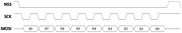
3W1L Display Interface [A0+8-bit]
3W1L interface in [A0+8-bit] mode, illustrated in the figure below, allows putting a total of 9 bits per transaction on the MOSI wire, in which
- First bit (“A0”) is the data-versus-command indicator bit.
- Next 8 bits (D7 through D0) are data bits.
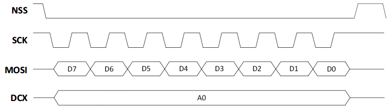
4W1L Display Interface [8-bit]
4W1L interface in [8-bit] mode, illustrated in the figure below, allows putting
- 8 bits per transaction on the MOSI wire, in which all bits (D7 through D0) are data bits.
- Data-versus-command information on the dedicated DCX wire, for the duration of the transfer.
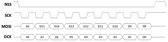
4W2L Display Interface [A0+8-bit]
4W2L interface in [A0+8-bit] mode, illustrated in the figure below, allows putting a total of 18 bits per transaction on the MOSI and DCX wires, in which
- First bit (“A0”) on both wires is the data-versus-command indicator bit. This bit is duplicated.
- Next 8 bits (D7 through D0) on MOSI wire are data bits.
- Next 8 bits (D15 through D8) on DCX wire are data bits.
Choice of DS and SPIMODE for Target Pixel Sizes
There are various choices of DS[4:0] and SPIMODE[1:0] when users desire to send pixels of a particular format. The choice mostly depends on the Display Module capabilities (number of wires and data lanes and pixel formats supported) and the desired level of performance (throughput).
The DMA transfer size, which is a setting outside of the DSPI IP, is also an important parameter, because it determines the granularity of data that is written into DSPI TX FIFO.
Typical choices of DS and SPIMODE for target pixel sizes are shown in 表 352. This table applies to 3 common pixel formats: RGB565, RGB666, and RGB888.
| Pixel Format | Pixel Size | Transfers per Pixel | DSPI Transfer Description | DMA Data Size DST_TR_WIDTH[2:0] | Transfer Mode SPIMODE[1:0] | DSPI Data size DS[4:0] |
|---|---|---|---|---|---|---|
| RGB565 | 16b | 2 | A0 + 8b on 1 lane | 0x0: 8 bits |
0x1: 3W1L | 0x07: 8 bits |
| 1 | A0 + 16b on 1 lane | 0x1: 16 bits | 0x1: 3W1L | 0x0F: 16 bits | ||
| 2 | 8b on 1 lane | 0x0: 8 bits | 0x2: 4W1L | 0x07: 8 bits | ||
| 1 | A0 + 8b on 2 lanes | 0x1: 16 bits | 0x3: 4W2L | 0x0F: 16 bits | ||
| RGB666 | 18b | 3 | A0 + 8b on 1 lane | 0x0: 8 bits | 0x1: 3W1L | 0x07: 8 bits |
| 2 | A0 + 9b on 1 lane | 0x1: 16 bits | 0x1: 3W1L | 0x08: 9 bits | ||
| 1 | A0 + 18b on 1 lane | 0x2: 32 bits | 0x1: 3W1L | 0x11: 18 bits | ||
| 3 | 8b on 1 lane | 0x0: 8 bits | 0x2: 4W1L | 0x07: 8 bits | ||
| 1 | A0 + 9b on 2 lanes | 0x2: 32 bits | 0x3: 4W2L | 0x11: 18 bits | ||
| RGB888 | 24b | 3 | A0 + 8b on 1 lane | 0x0: 8 bits | 0x1: 3W1L | 0x07: 8 bits |
| 1 | A0 + 24b on 1 lane | 0x2: 32 bits | 0x1: 3W1L | 0x17: 24 bits | ||
| 1 | A0 + 12b on 2 lanes | 0x2: 32 bits | 0x3: 4W2L | 0x17: 24 bits |
Registers
CTRL1
- Name: DSPI Control Register 1
- Description: This register specifies the configuration parameters of DSPI.
- Base Address: 0x4002E000
- Offset: 0x0
- Reset Value: 0x00000000
| Bits | Field Name | RW | Reset | Description |
|---|---|---|---|---|
31:16 |
RSVD |
R |
Reserved bits |
|
15 |
BIDIMODE |
RW |
0x0 |
Bidirectional data mode enable. This bit enables half-duplex communication using common single bidirectional data line. Keep RXONLY bit clear when bidirectional mode is active.
|
14 |
BIDIOE |
RW |
0x0 |
Output enable in bidirectional mode. This bit combined with the BIDIMODE bit selects the direction of transfer in bidirectional mode.
Note: This bit applies to MOSI pin. |
13 |
FPRST |
RW |
0x0 |
FIFO pointer reset This bit resets the pointers for TX FIFO and RX FIFO, works as a flush signal for both FIFOs. Any status flags related to RX FIFO and TX FIFO are also reset, as a result.
Note: After this bit is written with 1 to flush the FIFOs, it should be written with 0 to ensure normal operation. |
12:10 |
RSVD |
R |
Reserved bits |
|
9 |
SSM |
RW |
0x0 |
Software slave management When the SSM bit is set, the CS pin input is replaced with the value from the SSI bit.
|
8 |
SSI |
RW |
0x0 |
Internal slave select This bit takes effect only when the SSM bit is set. The value of this bit is forced onto the CS pin and the I/O. Value of the CS pin is ignored. |
7 |
RSVD |
R |
Reserved bit |
|
6 |
EN |
RW |
0x0 |
SPI enable
|
5:3 |
BR |
RW |
0x0 |
Baud rate control
Note: These bits should not be changed when communication is ongoing. |
2 |
MSTR |
RW |
0x0 |
Master selection
Note: This bit should not be changed when communication is ongoing. |
1 |
CPOL |
RW |
0x0 |
Clock polarity
Note: This bit should not be changed when communication is ongoing. For DSPI operation adopting MIPI DBI Type-C, only CPOL=1, CPHA=1 combination is relevant; other combinations should not be used. |
0 |
CPHA |
RW |
0x0 |
Clock phase
Note: This bit should not be changed when communication is ongoing. For DSPI operation adopting MIPI DBI Type-C, only CPOL=1, CPHA=1 combination is relevant; other combinations should not be used. |
CTRL2
- Name: DSPI Control Register 2
- Description: This register specifies the configuration parameters of DSPI.
- Base Address: 0x4002E000
- Offset: 0x04
- Reset Value: 0x0700
| Bits | Field Name | RW | Reset | Description |
|---|---|---|---|---|
31:13 |
RSVD |
R |
Reserved bits |
|
12:8 |
DS |
RW |
0x07 |
Data size These 5 bits configure the data length for SPI transfers:
For regular SPI transfers, typical DS values are 8-bit, 16-bit, and 32-bit. For display SPI transfers, typical DS values are 8-bit, 9-bit, 16-bit, 18-bit, and 24-bit. Note: If software attempts to write one of the “Not used” values, they are forced to be the value “0111” (8-bit). |
7 |
TXEIE |
RW |
0x0 |
TX buffer empty interrupt enable
Used to generate an interrupt request when the TXE flag is set. |
6 |
RSVD |
R |
Reserved bit |
|
5 |
ERRIE |
RW |
0x0 |
Error interrupt enable This bit controls the generation of an interrupt when an error condition occurs (OVR, MODF in SPI mode).
Note: This error will not occur in the current DSPI application. |
4 |
FRF |
RW |
0x0 |
Frame format
Note: This bit must be 0 at all times. |
3 |
CSP |
RW |
0x0 |
CS pulse management This bit is used in master mode only. It allows the SPI to generate a CS pulse between two pieces of consecutive data in continuous transfers. In the case of a single data transfer, it forces the CS pin high level after the transfer. It has no meaning if CPHA = ’1’, or FRF = ’1’.
Note: This bit must be written only when the SPI is disabled (SPE=0). |
2 |
SSOE |
RW |
0x0 |
SS output enable
Note: This bit must be 1 at all times. |
1 |
TXDMAEN |
RW |
0x0 |
Tx buffer DMA enable When this bit is set, a DMA request is generated whenever the TXE flag is set.
|
0 |
RSVD |
R |
Reserved bit |
STAT
- Name: DSPI Status Register
- Description: This register indicates the current working status of DSPI.
- Base Address: 0x4002E000
- Offset: 0x08
- Reset Value: 0x0002
| Bits | Field Name | RW | Reset | Description |
|---|---|---|---|---|
31:17 |
RSVD |
R |
0x0 |
Reserved bits |
16:13 |
FTLCNT |
RW |
0x0 |
TX FIFO count in units of bytes These bits are set and cleared by hardware.
|
12:9 |
RSVD |
R |
Reserved bits |
|
8 |
FRE |
RW |
0x0 |
Frame format error This flag is used for SPI in TI slave mode and I2S slave mode. [Not relevant] This flag is set by hardware and reset when DSPI_SR is read by software.
|
7 |
BUSY |
RW |
0x0 |
Busy flag
This flag is set and cleared by hardware. |
6 |
OVR |
RW |
0x0 |
Overrun flag
This flag is set by hardware and reset by a software sequence. Note: This error will not occur in the current DSPI application. |
5 |
MODF |
RW |
0x0 |
Mode fault
This flag is set by hardware and reset by a software sequence. Note: This error will not occur in the current DSPI application. |
4:2 |
RSVD |
R |
Reserved bits |
|
1 |
TXE |
RW |
0x0 |
Transmit buffer empty
|
0 |
RSVD |
R |
Reserved bit |
DATA
- Name: DSPI Data Register
- Description: This register is a write data register.
- Base Address: 0x4002E000
- Offset: 0x0C
- Reset Value: 0x0000
| Bits | Field Name | RW | Reset | Description |
|---|---|---|---|---|
31:0 |
DATA |
RW |
0x0 |
Data register Data to be transmitted Note: Data is always right-aligned. Unused bits are ignored when writing to the register. |
MODE
- Name: DSPI Display Mode Register
- Description: This register specifies the working mode parameters of DSPI.
- Base Address: 0x4002E000
- Offset: 0x10
- Reset Value: 0x0000
| Bits | Field Name | RW | Reset | Description |
|---|---|---|---|---|
31:3 |
RSVD |
R |
Reserved bits |
|
2 |
DCX |
RW |
0x0 |
Value of data-versus-command information used in Display SPI Protocol Modes. This bit specifies the value to put on the DCX wire of Display SPI interface or the “A0” value to use on the DOUT bit stream when this information is provided as part of the outgoing data bits.
|
1:0 |
SPIMODE |
RW |
0x0 |
SPI protocol mode This bit selects the SPI protocol mode.
|
