
PWM
Introduction
The device has two instances of Pulse Width Modulation (PWM) module. The PWM generates successive pulses with variable duty cycles that can be converted to analog levels by external discrete components, such as controlling LED brightness via a PWM signal.
Main Features
- Configurable output frequency and dynamic frequency configuration
- Three independent PWM channel outputs: pwma, pwmb, and pwmc
- Two operation modes: flicker mode and breath mode
- Two alignment modes: edge alignment mode and center alignment mode
- Configurable duty cycles in flicker mode
- Three configuration modes: synchronize-all, synchronize-separate, and asynchronous
- Polarity switching to support positive-drive and negative-drive mode
- Optional stop I/O voltage level in active/idle mode: low level or high level
Block Diagram
The PWM block diagram is illustrated in Figure 36.

Functional Description
The PWM module has two instances which are PWM0 and PWM1. There are two operation modes: flicker mode and breath mode. Each PWM instance can provide three independent channel outputs: pwma, pwmb and pwmc. Each channel shares the same frequency but can be configured with different duty cycles.
Bothpositive-drive mode and negative-drive mode are supported and can be configured by the DPENx field in the MODE register.
- In positive-drive mode, a valid output is configured by setting the PWM output logic level to 1, whereas an invalid output is set when the PWM output logic level is 0.
- In negative-drive mode, a valid output is configured by setting the PWM output logic level to 0, whereas an invalid output is set when PWM output logic level is 1.
Flicker Mode
In flicker mode, the PWM module outputs successive pulses with a certain frequency and duty as configured. PRD register is used to configure the frequency in the flicker mode. The duty of PWM can be configured in the range of 0% to 100% through CMPx0, CMPx1 and AQCTRL register. The three outputs can be configured independently, and they share one output frequency.

In flicker mode, if the stop level is configured (the default value of FLICKER_PAUSE_LEVEL_x is 0 when not set), the I/O level of the corresponding channel will be pulled to the set value when PWM stops.
Breath Mode
In breath mode, the duty of PWM output periodically changes from 0% to 100%, and then 100% to 0% uniformly. The breathing cycle can be set by the BRPRD register, which represents the number of PWM cycles required for the duty cycle 0%→100% and then 100%→0%.
A configurable duration of breath hold state (can be set by the HOLD rgister) is supported. The breath hold state is set between two adjacent breath processes, that is duty change (0%→100%→0%), breath hold, and duty change (0%→100%→0%). In the hold state, the PWM output is driven by inactive state.
In breath mode, the I/O levels of all channels are the same and set by the BREATH_PAUSE_LEVEL bit in the MODE register when PWM stops. When MCU enters sleep state, the stop level remains high in both flicker mode and breath mode.
Alignment
In flicker mode, both edge alignment and center alignment are supported through software approach.


Active Update
PWM module is capable of configuring output frequency dynamically. There are several shadow registers in the PWM module. The write operation will first change the shadow registers, and then will update the value of active registers from the shadow registers under certain conditions.
The configured data can be updated into active registers in three modes: synchronize-all mode (enabled by UPDATE.SA), synchronize-separate mode (enabled by UPDATE.SSCMPxx) and asynchronous update mode (enabled by UPDATE.SA and UPDATE.SSCMPxx).
Active registers update conditions:
-
In synchronize-all update mode (UPDATE.SA = 0x1), all effective registers of flicker mode or breath mode will be updated simultaneously. In flicker mode (MODE.BREATHEN = 0), after writing to PRD, the CMPxx and AQCTRL registers will update from shadow registers simultaneously when the Time Base counter counts to a value of PRD minus 1.
In breath mode (MODE.BREATHEN = 1), after writing to PRD, the BRPRD and HOLD registers will update from shadow registers simultaneously when the current breath process ends (the moment PWM duty reduces to 0%). When using the app_pwm_update_freq interface, the PWM frequency will be updated immediately.
-
In synchronize-separate update mode (UPDATE.SA = 0x0), the PRD, CMPxx, and AQCTRL registers will update when the Time Base counter counts to value of the PRD register minus 1, and if the corresponding UPDATE.SSCMPxx bit is set. The BRPRD and HOLD registers will update when the current breath process ends and the corresponding UPDATE.SSCMPxx bit is set.
- In asynchronous update mode (UPDATE.SA = 0x0 and UPDATE.SSCMPxx = 0x0), all registers will update instantly.
If the configurations need to be changed under synchronize-all update mode, CMPXX and AQCTRL in flicker mode, or HOLD in breath mode should be written before modifying the values of PRD and BRPRD.
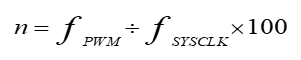
Duty Cycle Calculation
The PWM duty cycle can be configured as an integer from 0 to 100, depending on the following calculation formulas of the duty cycle accuracy "n".
- In edge-aligned mode:
- In center-aligned mode:
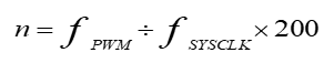
For example, when the clock frequency is 64 MHz, and the duty cycle is in the range of 0 to 100, the maximum PWM frequency can only be set to 640 kHz in the edge-aligned mode and 320 kHz in the center-aligned mode.
Recommended Setting in Breath Mode
In breath mode, in order to satisfy that the duty cycle of the waveform changes from 0 to 100 and then from 100 to 0, it is necessary to set the values of PRD and BRPRD to an integer that is multiple(s) of 128. The freq, bperiod and hperiod in the structure pwm_init_t need to meet the following formula during initialization:
where, k represents the number of PWM cycles required for the duty cycle from 0% to 100%; SYSCLK represents the system clock frequency; bperiod represents the breath period; hperiod represents the hold period.
Registers
MODE
- Name: Mode Register
- Description: This register sets the PWM operation mode.
- Base Address: 0x4000CB00 + x*0x100
- Offset: 0x0
- Reset Value: 0x00000000
*x is used to identify the PWM Module instance. The “x” can be 0 or 1.
| Bits | Field Name | RW | Reset | Description |
|---|---|---|---|---|
31:10 |
RSVD |
R |
Reserved bits |
|
9 |
BREATH_PAUSE_LEVEL |
RW |
0x0 |
PWMA/B/C output IO level when suspending in Breath Mode |
8 |
FLIKCER_PAUSE_LEVEL_C |
RW |
0x0 |
PWMC output IO level when suspending in Flicker Mode |
7 |
FLIKCER_PAUSE_LEVEL_B |
RW |
0x0 |
PWMB output IO level when suspending in Flicker Mode |
6 |
FLIKCER_PAUSE_LEVEL_A |
RW |
0x0 |
PWMA output IO level when suspending in Flicker Mode |
5 |
DPENC |
RW |
0x0 |
Enable PWMC positive-drive mode. Value:
|
4 |
DPENB |
RW |
0x0 |
Enable PWMB positive-drive mode. Value:
|
3 |
DPENA |
RW |
0x0 |
Enable PWMA positive-drive mode. Value:
|
2 |
BREATHEN |
RW |
0x0 |
Enable Breath mode. Value:
|
1 |
PAUSE |
RW |
0x0 |
PWM pause signal. Value:
|
0 |
EN |
RW |
0x0 |
Enable PWM. Value:
|
UPDATE
- Name: Update Register
- Description: This register is used to set the synchronous update mode.
- Base Address: 0x4000CB00 + x*0x100
- Offset: 0x4
- Reset Value: 0x00000000
| Bits | Field Name | RW | Reset | Description |
|---|---|---|---|---|
31:18 |
RSVD |
R |
Reserved bits |
|
17 |
SSAQCTRL | RW |
0x0 |
Enable separate update of AQCTRL. Value:
|
16 |
SSHOLD | RW |
0x0 |
Enable separate update of HOLD. Value:
|
15 |
SSBRPRD | RW |
0x0 |
Enable separate update of BRPRD. Value:
|
14 |
SSCMPC1 | RW |
0x0 |
Enable separate update of CMPC1. Value:
|
13 |
SSCMPC0 | RW |
0x0 |
Enable separate update of CMPC0. Value:
|
12 |
SSCMPB1 | RW |
0x0 |
Enable separate update of CMPB1. Value:
|
11 |
SSCMPB0 | RW |
0x0 |
Enable separate update of CMPB0. Value:
|
10 |
SSCMPA1 | RW |
0x0 |
Enable separate update of CMPA1. Value:
|
9 |
SSCMPA0 | RW |
0x0 |
Enable separate update of CMPA0. Value:
|
8 |
SSPRD | RW |
0x0 |
Enable separate update of PRD. Value:
|
7:2 |
RSVD |
R |
Reserved bits |
|
1 |
SA | RW |
0x0 |
Enable synchronous update. Value:
|
0 |
SAG | R |
0x0 |
Synchronous update ongoing Value:
|
PRD
- Name: Period Register
- Description: This register is used to set the PWM cycle.
- Base Address: 0x4000CB00 + x*0x100
- Offset: 0x8
- Reset Value: 0x00000064
| Bits | Field Name | RW | Reset | Description |
|---|---|---|---|---|
31:0 |
PRD |
RW |
0x64 |
The period of PWM output, PRD=fCLK/fPWM |
CMPA0
- Name: Compare A0 Register
- Description: This register controls the PWM duty of Compare register 0 of channel A.
- Base Address: 0x4000CB00 + x*0x100
- Offset: 0xC
- Reset Value: 0x00000000
| Bits | Field Name | RW | Reset | Description |
|---|---|---|---|---|
31:0 |
CMPA0 |
RW |
0x0 |
PWMA duty control register0 |
CMPA1
- Name: Compare A1 Register
- Description: This register controls the PWM duty of Compare register 1 of channel A.
- Base Address: 0x4000CB00 + x*0x100
- Offset: 0x10
- Reset Value: 0x00000000
| Bits | Field Name | RW | Reset | Description |
|---|---|---|---|---|
31:0 |
CMPA1 |
RW |
0x0 |
PWMA duty control register1 |
CMPB0
- Name: Compare B0 Register
- Description: This register controls the PWM duty of Compare register 0 of channel B.
- Base Address: 0x4000CB00 + x*0x100
- Offset: 0x14
- Reset Value: 0x00000000
| Bits | Field Name | RW | Reset | Description |
|---|---|---|---|---|
31:0 |
CMPB0 |
RW |
0x0 |
PWMB duty control register0 |
CMPB1
- Name: Compare B1 Register
- Description: This register controls the PWM duty of Compare register 1 of channel B.
- Base Address: 0x4000CB00 + x*0x100
- Offset: 0x18
- Reset Value: 0x00000000
| Bits | Field Name | RW | Reset | Description |
|---|---|---|---|---|
31:0 |
CMPB1 |
RW |
0x0 |
PWMB duty control register1 |
CMPC0
- Name: Compare C0 Register
- Description: This register controls the PWM duty of Compare register 0 of channel C.
- Base Address: 0x4000CB00 + x*0x100
- Offset: 0x1C
- Reset Value: 0x00000000
| Bits | Field Name | RW | Reset | Description |
|---|---|---|---|---|
31:0 |
CMPC0 |
RW |
0x0 |
PWMC duty control register0 |
CMPC1
- Name: Compare C1 Register
- Description: This register controls the PWM duty of Compare register 1 of channel C.
- Base Address: 0x4000CB00 + x*0x100
- Offset: 0x20
- Reset Value: 0x00000000
| Bits | Field Name | RW | Reset | Description |
|---|---|---|---|---|
31:0 |
CMPC1 |
RW |
0x0 |
PWMC duty control register1 |
AQCTRL
- Name: Action Qualifier Control Register
- Description: This register is used to set actions when counter reaches the compare value.
- Base Address: 0x4000CB00 + x*0x100
- Offset: 0x24
- Reset Value: 0x00000000
| Bits | Field Name | RW | Reset | Description |
|---|---|---|---|---|
31:12 |
RSVD |
R |
Reserved bits |
|
11:10 |
C1 |
RW |
0x0 |
Action of event CNT_CMPC1 control register Value:
|
9:8 |
C0 |
RW |
0x0 |
Action of event CNT_CMPC0 control register Value:
|
7:6 |
B1 |
RW |
0x0 |
Action of event CNT_CMPB1 control register Value:
|
5:4 |
B0 |
RW |
0x0 |
Action of event CNT_CMPB0 control register Value:
|
3:2 |
A1 |
RW |
0x0 |
Action of event CNT_CMPA1 control register Value:
|
1:0 |
A0 |
RW |
0x0 |
Action of event CNT_CMPA0 control register Value:
|
BRPRD
- Name: Breath Period Register
- Description: This register configures the period of breath mode.
- Base Address: 0x4000CB00 + x*0x100
- Offset: 0x28
- Reset Value: 0x00000000
| Bits | Field Name | RW | Reset | Description |
|---|---|---|---|---|
31:0 |
BRPRD |
RW |
0x0 |
Register for breath period that is the required time (number of clock) that the duty changes from 0% to 100% in breath mode. |
HOLD
- Name: Hold Register
- Description: This register configures the hold period in breath mode.
- Base Address: 0x4000CB00 + x*0x100
- Offset: 0x2C
- Reset Value: 0x00000000
| Bits | Field Name | RW | Reset | Description |
|---|---|---|---|---|
31:24 |
RSVD |
R |
Reserved bits |
|
23:0 |
HOLD |
RW |
0x0 |
Breath hold control register. The value should be the required number of clock in breath hold state. |
