Power Consumption
The software constantly adjusts the power supplies of the power management modules (such as DC-DC/LDO) according to different temperatures and system clock sources, so estimating the current consumption of an application can be challenging when the measurements cannot be performed directly on different test conditions. To facilitate the estimation, a set of current consumption scenarios are provided to show the typical current drawn from the VBATL supply.
Each scenario specifies a set of operations and conditions to apply to the given scenario. All scenarios are listed in "Electrical Specifications". The table below shows a set of common conditions used in all scenarios, unless otherwise stated in the description of a given scenario.
| Condition | State | Remark |
|---|---|---|
| Supply | VBAT = 3.3 V | |
| Temperature | 25°C | |
| CPU | WFI/WFE | |
| Peripheral | All idle | |
| Clock | System clock = 64 MHz@HFRC, low clock = 32.768 kHz@LFXO_32K | |
| Flash clock | 64 MHz | |
| Core RAM | Full 96 KB retention | In active mode, full 96 KB RAM is powered; in sleep mode, full 96 KB RAM is retained. |
| Cache enabled | Yes, 4-way associative | Only applied when the CPU is running from Flash memory. |
| Bluetooth LE Stack | Disabled | |
| 32 MHz crystal | 32 MHz | Only applied when the high-frequency crystal oscillator (HFXO_32M) is running, and HFXO_32M is used when the radio is running. |
| 32 KHz crystal | 32.768 KHz | Only applied when the low-frequency crystal oscillator (LFXO_32K) is running. |
| BOD/IO_LDO | BOD Enabled/IO_LDO On | |
| VDDIO | 3.3 V | |
| DC-DC/CORE_LDO | DC-DC = 1.05 V / CORE_LDO = 0.90 V | |
| Regulator | DC-DC | |
| Flash | Standby mode | In active mode, Flash is powered on; in sleep mode, Flash is powered off. |
| Inductors | ||
| Compiler version | MDK-ARM Plus Version: 5.26.2.0 | |
| Compiler flag | --C99 -c --cpu Cortex-M4F.fp -D__MICROLIB --li -g -O3 --apcs=interwork --split_sections -D__UVISION_VERSION="526" |
Electrical Specifications
The current consumption data listed in the following tables is applicable to all devices and is obtained under the common conditions in 表 38, unless otherwise stated.
The minimum and maximum values in the following tables represent the worst conditions across process variation at TA = 25°C.
Sleep Current Consumption
| Symbol | Condition1 | Condition2 | Condition3 | Min. | Typ. | Max. | Unit |
|---|---|---|---|---|---|---|---|
| IUDS,RAM_OFF, RESET | Ultra deep sleep mode | No RAM retention | Woken up on reset | 1.9 | μA | ||
| IUDS,RAM_OFF, AON_GPIO | Woken up on AON GPIO | 1.9 | μA | ||||
| IUDS,RAM_OFF,SLP_TIMER | Woken up on Sleep Timer | 1.9 | μA | ||||
| IUDS,RAM_OFF,SLP_TIMER_LFRC | Woken up on Sleep Timer (running from LFRC_32K clock) | 1.9 | μA | ||||
| IS,RAM_OFF,ANY | Sleep mode | Woken up on any events | 2.2 | μA | |||
| IS,RAM48K_RET,BLE | Full 48 KB RAM retention | Woken up on Bluetooth LE controller | 2.6 | μA | |||
| IS,RAM96K_RET,BLE | Full 96 KB RAM retention | Woken up on Bluetooth LE controller | 2.8 | μA | |||
| IS,RAM96K_RET,BLE_LFRC | Woken up on Bluetooth LE controller (running from LFRC_32K clock) | 2.8 | μA | ||||
| IS,RAM96K_RET,SLP_TIMER | Woken up on sleep timer | 2.8 | μA | ||||
| IS,RAM96K_RET,COMP | Woken up on LPCOMP | 3.0 | μA | ||||
| IS,RAM96K_RET,SLP_TIMER_LFRC | Woken up on sleep timer (running from LFRC_32K clock) | 2.8 | μA | ||||
| IS,RAM96K_RET,RTC | Woken up on RTC | 2.8 | μA |
MCU Current Consumption
| Symbol | Condition1 | Condition2 | Condition3 | Min. | Typ. | Max. | Unit |
|---|---|---|---|---|---|---|---|
| ICOREMARK | CPU running CoreMark from Flash | 3.0 | mA | ||||
| ICOREMARK,SYS_LDO | Regulator = SYS_LDO | 4.1 | mA | ||||
| ICOREMARK,64M_HFXO | System clock = 64 MHz from HFXO clock | 3.8 | mA | ||||
| ICOREMARK,16M_HFRC | System clock = 16 MHz from HFRC clock | 1.3 | mA | ||||
| ILOOP | CPU running while loop from Flash | 2.5 | mA | ||||
| ILOOP,SYS_LDO | Regulator = SYS_LDO | 3.4 | mA | ||||
| ILOOP,64M_HFXO | System clock = 64 MHz from HFXO clock | 3.2 | mA | ||||
| IIDLE | CPU idle | 1.4 | mA | ||||
| IIDLE,SYS_LDO | Regulator = SYS_LDO | 2.0 | mA | ||||
| IIDLE,64M_HFXO | System clock = 64 MHz from HFXO clock | 2.2 | mA |
| Symbol | Condition1 | Condition2 | Condition3 | Min. | Typ. | Max. | Unit |
|---|---|---|---|---|---|---|---|
| ICOREMARK | CPU running CoreMark from Flash | 2.0 | mA | ||||
| ICOREMARK,SYS_LDO | Regulator = SYS_LDO | 4.2 | mA | ||||
| ICOREMARK,64M_HFXO | System clock = 64 MHz from HFXO clock | 2.5 | mA | ||||
| ICOREMARK,16M_HFRC | System clock = 16 MHz from HFRC clock | 0.9 | mA | ||||
| ILOOP | CPU running while loop from Flash | 1.8 | mA | ||||
| ILOOP,SYS_LDO | Regulator = SYS_LDO | 3.6 | mA | ||||
| ILOOP,64M_HFXO | System clock = 64 MHz from HFXO clock | 2.3 | mA | ||||
| IIDLE | CPU idle | 1.2 | mA | ||||
| IIDLE,SYS_LDO | Regulator = SYS_LDO | 2.2 | mA | ||||
| IIDLE,64M_HFXO | System clock = 64 MHz from HFXO clock | 1.7 | mA |
Radio Current Consumption
GR533x family members support different power amplifiers for optimal power performance:
- GR5331: ultra-low power amplifier (UPA, -15 dBm to 2 dBm), and small power amplifier (SPA, -20 dBm to 6 dBm)
- GR5332: small power amplifier (SPA, -20 dBm to 5 dBm), and high power amplifier (HPA, -10 dBm to 15 dBm)
Where UPA uses a different matching network circuit, compared with other power amplifiers, to achieve the lowest power consumption.
Please refer to the Bill of Materials of the specific GR533x member for tailored recommendations, including tolerance, component size, recommended manufacturer, and recommended part number.
Radio Transmitting Current Consumption for GR5332
| Symbol | Condition 1 | Condition 2 | Condition 3 | Min. | Typ. | Max. | Unit |
|---|---|---|---|---|---|---|---|
| ITRANSMIT,0dBm,SPA,1Mbps,HFXO16M | 1 Mbps Bluetooth LE, SPA, System clock = 16 MHz from HFXO clock |
Radio transmitting @0 dBm output power | 5.9 | mA | |||
| ITRANSMIT,0dBm,SPA,1Mbps,HFXO64M | 1 Mbps Bluetooth LE, SPA, System clock = 64 MHz from HFXO clock |
6.3 | mA | ||||
| ITRANSMIT,0dBm,SPA,1Mbps,HFXO64M,SYS_LDO | Regulator = SYS_LDO | 15.5 | mA | ||||
| ITRANSMIT,4dBm,SPA,1Mbps,HFXO64M | Radio transmitting @4 dBm output power | 7.7 | mA | ||||
| ITRANSMIT,4dBm,SPA,1Mbps,HFXO64M,SYS_LDO | Regulator = SYS_LDO | 19 | mA | ||||
| ITRANSMIT,-20dBm,SPA,1Mbps,HFXO64M | Radio transmitting @-20 dBm output power | 3.3 | |||||
| ITRANSMIT,4dBm,HPA,1Mbps,HFXO64M,SYS_LDO | 1Mbps Bluetooth LE, HPA, System clock = 64 MHz from HFXO clock |
Regulator = SYS_LDO | Radio transmitting @4 dBm output power | 33.5 | mA | ||
| ITRANSMIT,15dBm,HPA,1Mbps,HFXO64M,SYS_LDO | Radio transmitting @15 dBm output power | 86.3 | mA | ||||
| ITRANSMIT,-10dBm,HPA,1Mbps,HFXO64M,SYS_LDO | Radio transmitting @-10 dBm output power | 16 | mA |
Radio Transmitting Current Consumption for GR5331
| Symbol | Condition 1 | Condition 2 | Min. | Typ. | Max. | Unit |
|---|---|---|---|---|---|---|
| ITRANSMIT,0dBm,UPA,1Mbps,HFXO16M | 1 Mbps Bluetooth LE, UPA, System clock = 16 MHz from HFXO clock |
Radio transmitting @0 dBm output power | 5.7 | mA | ||
| ITRANSMIT,0dBm,UPA,1Mbps,HFXO64M | 1 Mbps Bluetooth LE, UPA, System clock = 64 MHz from HFXO clock |
6.2 | mA | |||
| ITRANSMIT, -15dBm,UPA,1Mbps,HFXO64M | Radio transmitting @-15 dBm output power | 4.5 | mA | |||
| ITRANSMIT,0dBm,SPA,1Mbps,HFXO16M | 1 Mbps Bluetooth LE, SPA, System clock = 16 MHz from HFXO clock |
Radio transmitting @0 dBm output power | 7.7 | mA | ||
| ITRANSMIT,0dBm,SPA,1Mbps,HFXO64M | 1 Mbps Bluetooth LE, SPA, System clock = 64 MHz from HFXO clock |
8.2 | mA | |||
| ITRANSMIT,5dBm,SPA,1Mbps,HFXO64M | Radio transmitting @5 dBm output power | 12.1 | mA | |||
| ITRANSMIT, -20dBm,SPA,1Mbps,HFXO64M | Radio transmitting @-20 dBm output power | 5.0 | mA |
| Symbol | Condition 1 | Condition 2 | Min. | Typ. | Max. | Unit |
|---|---|---|---|---|---|---|
| ITRANSMIT,0dBm,UPA,1Mbps,HFXO16M | 1 Mbps Bluetooth LE, UPA, System clock = 16 MHz from HFXO clock |
Radio transmitting @0 dBm output power | 3.8 | mA | ||
| ITRANSMIT,0dBm,UPA,1Mbps,HFXO64M | 1 Mbps Bluetooth LE, UPA, System clock = 64 MHz from HFXO clock |
4.1 | mA | |||
| ITRANSMIT,-15dBm,UPA,1Mbps,HFXO64M | Radio transmitting @-15 dBm output power | 3.1 | mA | |||
| ITRANSMIT,0dBm,SPA,1Mbps,HFXO16M | 1 Mbps Bluetooth LE, SPA, System clock = 16 MHz from HFXO clock |
Radio transmitting @0 dBm output power | 5.0 | mA | ||
| ITRANSMIT,0dBm,SPA,1Mbps,HFXO64M | 1 Mbps Bluetooth LE, SPA, System clock = 64 MHz from HFXO clock |
5.3 | mA | |||
| ITRANSMIT,5dBm,SPA,1Mbps,HFXO64M | Radio transmitting @5 dBm output power | 7.9 | mA | |||
| ITRANSMIT, -20dBm,SPA,1Mbps,HFXO64M | Radio transmitting @-20 dBm output power | 3.4 | mA |
Radio Receiving Current Consumption for GR5332
| Symbol | Condition 1 | Condition 2 | Condition 3 | Min. | Typ. | Max. | Unit |
|---|---|---|---|---|---|---|---|
| IRECEIVE,1Mbps,64M_HFXO | Radio receiving @ 1 Mbps Bluetooth LE mode | System Clock = 64 MHz from HFXO clock | 5.2 | mA | |||
| IRECEIVE,1Mbps,16M_HFXO | System Clock = 16 MHz from HFXO clock | 4.9 | mA | ||||
| IRECEIVE,1Mbps,SYS_LDO, 64M_HFXO | Regulator = SYS_LDO | System Clock = 64 MHz from HFXO clock | 12.8 | mA | |||
| IRECEIVE,1Mbps,SYS_LDO,16M_HFXO | System Clock = 16 MHz from HFXO clock | 12.0 | mA |
Radio Receiving Current Consumption for GR5331
| Symbol | Condition 1 | Condition 2 | Min. | Typ. | Max. | Unit |
|---|---|---|---|---|---|---|
| IRECEIVE,1Mbps,64M_HFXO | Radio receiving @ 1 Mbps Bluetooth LE mode | System clock = 64 MHz from HFXO clock | 8.5 | mA | ||
| IRECEIVE,1Mbps,16M_HFXO | System clock = 16 MHz from HFXO clock | 7.3 | mA |
| Symbol | Condition 1 | Condition 2 | Min. | Typ. | Max. | Unit |
|---|---|---|---|---|---|---|
| IRECEIVE,1Mbps,64M_HFXO | Radio receiving @ 1 Mbps Bluetooth LE mode | System clock = 64 MHz from HFXO clock | 5.0 | mA | ||
| IRECEIVE,1Mbps,16M_HFXO | System clock = 16 MHz from HFXO clock | 4.7 | mA |
ADC Current Consumption
| Symbol | Condition 1 | Condition 2 | Min. | Typ. | Max. | Unit |
|---|---|---|---|---|---|---|
| IADC,4KHz,128_POINTS | CPU running, acquiring 128 points | ADC sampling@4 kHz sample clock | 120 | uA | ||
| IADC,16KHz,128_POINTS | ADC sampling@16 kHz sample clock | 120 | uA | |||
| IADC,1MHz,128_POINTS | ADC sampling@1 MHz sample clock | 120 | uA | |||
| IADC,16MHz,128_POINTS | ADC sampling@16 MHz sample clock | 120 | uA |
TEMP Current Consumption
| Symbol | Condition | Min. | Typ. | Max. | Unit |
|---|---|---|---|---|---|
| ITEMP | TEMP measurement started | TBD | mA |
VBAT Current Consumption
| Symbol | Condition | Min. | Typ. | Max. | Unit |
|---|---|---|---|---|---|
| IVBAT | VBAT measurement started | TBD | mA |
COMP Current Consumption
| Symbol | Condition | Min. | Typ. | Max. | Unit |
|---|---|---|---|---|---|
| ICOMP | COMP started | 0.2 | μA |
BOD Current Consumption
| Symbol | Condition | Min. | Typ. | Max. | Unit |
|---|---|---|---|---|---|
| IBOD,Reset | BOD running | 200 | nA | ||
| IBOD,Interrupt | BOD interrupt enabled | 50 | nA |
TRNG Current Consumption
| Symbol | Condition | Min. | Typ. | Max. | Unit |
|---|---|---|---|---|---|
| ITRNG | TRNG running | TBD | μA |
DMA Current Consumption
| Symbol | Condition | Min. | Typ. | Max. | Unit |
|---|---|---|---|---|---|
| IDMA,M2M | DMA running, memory to memory | TBD | μA |
Typical Current Curves
Typical current curves indicate typical current under the conditions as stated below.
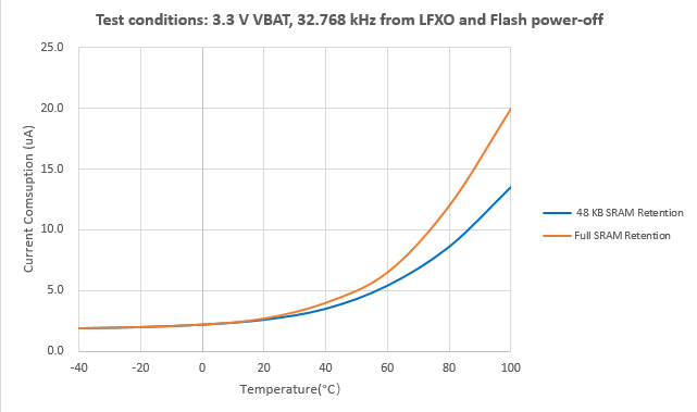
Sleep Mode
Typical conditions: VBAT = 3.3 V, system clock = 32.768 kHz@LFXO, Flash power-off.
The figure below shows the typical current curves of the device in sleep mode with different SRAM retention modes.
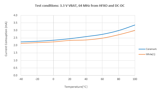
Active Mode
Typical conditions: VBAT = 3.3 V, system clock = 64 MHz@HFXO, regulator = DC-DC.
The figure below shows the typical current curves of the device in active mode (Coremark vs. While(1)) with various temperatures.
Radio Transmission
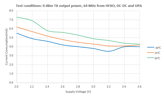
Radio Transmitting @ 0dBm Output Power for GR5331
Typical conditions: system clock = 64 MHz @HFXO, regulator = DC-DC, RF power amplifier = UPA.
The figure below shows the typical current curves of the GR5331 at 0 dBm TX output power, with various supply voltages and temperatures.
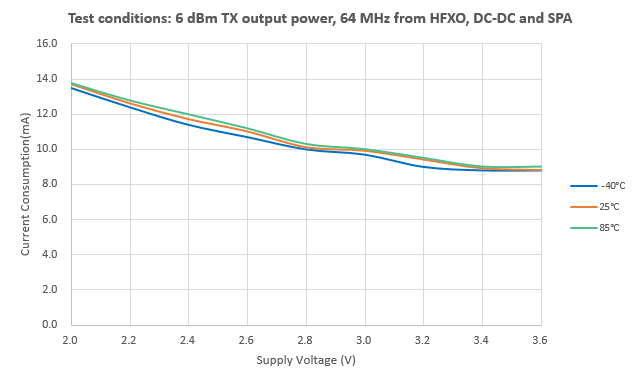
Radio Transmitting @ 6dBm Output Power for GR5331
Typical conditions: system clock = 64 MHz @HFXO, regulator = DC-DC, RF power amplifier = SPA.
The figure below shows the typical current curves of the GR5331 at 6 dBm TX output power, with various supply voltages and temperatures.
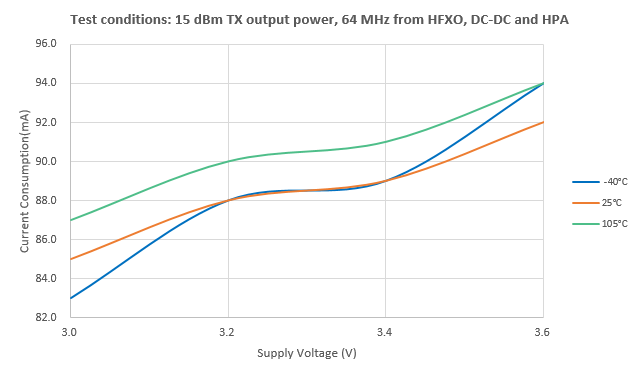
Radio Transmitting @ 15dBm Output Power for GR5332
Typical conditions: System clock = 64 MHz @HFXO, regulator = SYS_LDO, RF power amplifier = HPA.
The figure below shows the typical current curves of the GR5332 at 15 dBm TX output power, considering various supply voltages and temperatures.