
UART
Introduction
The device has two instances of Universal Asynchronous Receiver/Transmitter (UART) module. The UART complies with the industry-standard 16550. All the two UART instances support full duplex asynchronous serial communication with hardware flow control. The register address space is relocated to 32-bit data boundaries for Advance Peripheral Bus (APB) implementation
Main Features
-
Full-duplex asynchronous communications
-
Programmable character properties
-
Transmit and receive FIFO depth at 16 bytes
-
Hardware flow control support
-
DMA support
-
IrDA SIR support
-
Two UART instances
Block Diagram
The functional block diagram of UART is shown as below.

The following description illustrates each of the major blocks shown in the figure above.
-
Reset Block resets the clock domain.
-
APB Interface connects to APB bus.
-
Register Block is responsible for the main UART functionality including control, status, and interrupt generation.
-
Modem Sync Block synchronizes the modem input signal.
-
FIFO Block (optional) is responsible for FIFO control and storage — when using internal RAM — or optionally signaling to control external RAM.
-
Sync Block (optional) is implemented when the peripheral is configured to have a separate serial data clock (known as two-clock implementation).
-
Timeout Detector Block (optional) indicates the absence of character data movement in the receiver FIFO within a given time period; this is used to generate character timeout interrupts when enabled. This block can also have optional clock gate enable outputs — uart_lp_req_pclk for single clock implementations or uart_lp_req_pclk and uart_lp_req_sclk for two-clock implementations — in order to indicate:
-
TX and RX pipelines are cleared; that is, there is no data.
-
No activity has occurred.
-
Modem control input signals have not changed within a given time period.
-
-
Baud Clock Generator produces the transmitter and receiver baud clock along with the output reference clock signal (baudout_n).
-
Serial Transmitter converts the parallel data — written to the UART — into serial form and adds all additional bits, as specified by the control register, for transmission.
-
Serial UART
-
IrDA 1.0 SIR
-
-
Serial Receiver converts the serial data character — specified by the control register — received in UART form. This block controls:
-
Parity error detection
-
Framing error detection
-
Line break detection
-
Functional Description
UART (RS232) Serial Protocol
-
The serial communication between the UART and a selected device is asynchronous, so additional start and stop bits are added to the serial data to indicate the beginning and end. Utilizing these bits allows two devices to be synchronized. This structure of serial data, accompanied by start and stop bits, is referred to as a character, as shown below.
图 52 Timing diagram -
An additional parity bit can be added to the serial character. This bit appears after the last data bit and before the stop bit(s) in the character structure in order to provide the UART with the ability to perform simple error checking on the received data.
-
The UART Line Control Register (LCR) is used to control the serial character characteristics. The individual bits of the data word are sent after the start bit, starting with the least significant bit (LSB). These are followed by the optional parity bit, followed by the stop bit(s), which can be 1, 1.5, or 2.
-
All the bits in the transmission are transmitted for exactly the same time duration; the exception to this is the half-stop bit when 1.5 stop bits are used. This duration is referred to as a Bit Period or Bit Time; one Bit Time equals sixteen baud clocks.
-
To ensure stability on the line, the receiver samples the serial input data at approximately the midpoint of the Bit Time once the start bit has been detected. The exact number of baud clocks that are transmitted by each bit is known, so calculating the midpoint for sampling is not difficult; the midpoint for sampling occurs every sixteen baud clocks after sampling is performed at the midpoint of the start bit.
-
Together with serial input debouncing, this sampling helps to avoid the detection of false start bits. Short glitches are filtered out by debouncing, and no transition is detected on the line. If a glitch is wide enough to avoid filtering by debouncing, a falling edge is detected. However, a start bit is detected only if the line is again sampled low after half a Bit Time has elapsed. The following figure shows the sampling points of the first two bits in a serial character.
图 53 Receiver serial data sample points -
As part of the 16550 standard, an optional baud clock reference output signal (baudout_n) provides timing information for receiving devices that require it. The baud rate of the UART is controlled by the serial clock – sclk or pclk in a single clock implementation – and the Divisor Latch Register (DLH and DLL).
-
Serial data baud rate can be calculated as follows: Baud rate = (System clock frequency)/(16*Divisor). The Divisor is composed of an integer part (DLH/DLL register) and a fractional part (4-bit DLF register).
Fractional Baud Rate Support
UART supports fractional baud rate that enables users to program the fractional part of the divisor value to generate a fractional baud rate that results in reduced frequency error. The baud rate of UART is controlled by sclk in asynchronous serial clock implementation or pclk in single clock implementation and the Divisor Latch Register (DLH and DLL).
The baud rate is determined by the following factors:
-
Serial clock operating frequency (sclk in asynchronous serial clock implementation or pclk in single clock implementation)
-
The desired baud rate, or Baud rate (selected)
-
The baud rate generator divisor value, DIVISOR (composed of DLH & DLL registers).
-
The acceptable baud-rate error: Percentage ERROR.
The equation to calculate the baud rate is as follows:
where
DIVISOR – Number (in hexadecimal) to program the DLL and DLH, which represents the Baud rate divisor. Serial clock operating frequency – Frequency at sclk pin of UART. The Error between the Baud rate and Baud rate (selected) is given as:
When configuring the UART for Fractional Baud Rate, pay attention to the following formula: (Divisor Fraction value, DLF.DLF)/(2^DLF_SIZE).
The following table shows fractional values when the DLF_SIZE=4.
| DLF Value | Fraction | Fractional Value |
|---|---|---|
| 0000 | 0/16 | 0.0000 |
| 0001 | 1/16 | 0.0625 |
| 0010 | 2/16 | 0.125 |
| 0011 | 3/16 | 0.1875 |
| 0100 | 4/16 | 0.25 |
| 0101 | 5/16 | 0.3125 |
| 0110 | 6/16 | 0.375 |
| 0111 | 7/16 | 0.4375 |
| 1000 | 8/16 | 0.5 |
| 1001 | 9/16 | 0.5625 |
| 1010 | 10/16 | 0.625 |
| 1011 | 11/16 | 0.6875 |
| 1100 | 12/16 | 0.75 |
| 1101 | 13/16 | 0.8125 |
| 1110 | 14/16 | 0.875 |
| 1111 | 15/16 | 0.9375 |
The programmable fractional baud rate divisor enables a finer resolution of baud clock than the conventional integer divider. The programmable fractional baud clock divider allows for the programmability of both an integer divisor as well as fractional component. The average frequency of the baud clock from the fractional baud rate divisor is dependent upon both the integer divisor and the fractional component, thereby providing a finer resolution to the average frequency of the baud clock.
where
BRDI: Integer part of the divisor, with high bytes programmed by the DLH and low bytes programmed by the DLL.
BRDF: Fractional part of the divisor, which is programmed by the DLF.
FIFO Support
The UART module provides two 16-byte FIFO submodules: one (UART TX FIFO) for transmission and one (UART RX FIFO) for reception. By configuring the Shadow RCVR Trigger (SRT) register, you can program the trigger level in the RX FIFO at which the Received Data Available Interrupt is generated. By configuring the Shadow TX Empty Trigger (STET) register, you can program the trigger level in the TX FIFO at which the Empty Threshold Reached Interrupt is generated.
Interrupts
Assertion of the UART interrupt output signal occurs whenever one of the several prioritized interrupt types are enabled and active. When an interrupt occurs, the master accesses the IIR register. The following interrupt types can be enabled with the IER register:
-
Receiver Error
-
Receiver Data Available
-
Character Timeout (in FIFO mode only)
-
Transmitter Holding Register Empty at/below threshold (in Programmable THRE interrupt mode)
-
Modem Status
-
Busy Detect Indication
These interrupt types are explained in detail in the table below.
| Interrupt ID | Interrupt Set and Reset Functions | |||
|---|---|---|---|---|
| Bit3 Bit2 Bit1 Bit0 | Priority Level | Interrupt Type | Interrupt Source | Interrupt Reset Control |
| 0 0 0 1 | - | None | None | - |
| 0 1 1 0 | Highest | Receiver line status | Overrun/Parity/Framing errors, break interrupt, or address received interrupt | For overrun/parity/framing/break interrupt reset control, the behavior is as follows: The status is cleared on:
|
| 0 1 0 0 | Second | Received data available | Receiver data available (non-FIFO mode or FIFOs disabled) or RCVR FIFO trigger level reached (FIFO mode and FIFOs enabled) | Reading the receiver buffer register (non-FIFO mode or FIFOs disabled) or the FIFO increases above the trigger level (FIFO mode and FIFOs enabled). |
| 1 1 0 0 | Second | Character time indication | No characters in or out of the RCVR FIFO during the last 4 character times and there is at least 1 character in it during this time | Reading the receiver buffer register |
| 0 0 1 0 | Third | Transmit holding register empty | Transmitter holding register empty (Prog. THRE Mode disabled) or XMIT FIFO at or below threshold (Prog. THRE Mode enabled) | Reading the IIR register (if source of interrupt); or, writing into THR (FIFOs or THRE Mode not selected or disabled) or XMIT FIFO above threshold (FIFOs and THRE Mode selected and enabled) |
| 0 0 0 0 | Fourth | Modem status | Clear to send or data set ready or ring indicator or data carrier detect. Note: If auto flow control mode is enabled, a change in Clear to Send (CTS) (that is, DCTS set) does not cause an interrupt. |
Reading the Modem status register |
| 0 1 1 1 | Fifth | Busy detect indication | UART_16550_COMPATIBLE = NO and master has tried to write to the Line Control Register while the DW_apb_uart is busy (USR[0] is set to 1) | Reading the UART status register |
Auto Flow Control
The UART can be configured to have a 16750-compatible Auto Request to Send (RTS) and Auto Clear To Send (CTS) serial data flow control mode available; if FIFOs are not implemented, this mode cannot be selected. When Auto Flow Control is not selected, none of the corresponding logics is implemented, and the mode cannot be enabled, reducing overall gate counts. When Auto Flow Control mode is selected, it can be enabled with the Modem Control Register (MCR[5] = 1).
The figure below shows a block diagram of the Auto Flow Control functionality.

Auto RTS and Auto CTS are described as follows:
-
Auto RTS becomes active when all the following conditions occur:
-
Auto Flow Control is selected during configuration
-
FIFOs are implemented
-
RTS (Both MCR[1] bit and MCR[5] bit are set)
-
FIFOs are enabled (FCR[0]) bit is set)
When Auto RTS is enabled, the rts_n output is forced inactive (high) when the FIFO is almost full, where “almost full” refers to two available slots in the FIFO. When rts_n is connected to the cts_n input of another UART device, the other UART stops sending serial data until the receiver FIFO has available space; that is, until it is completely empty.
The selectable receiver FIFO threshold values are:
- 1
- 1/4
- 1/2
- 2 less than full
Because one additional character can be transmitted to the UART after rts_n has become inactive—due to data already having entered the transmitter block in the other UART— setting the threshold to “2 less than full” allows maximum use of the FIFO with a safety zone of one character.
Ten receiver FIFO becomes completely empty by reading the Receiver Buffer Register (RBR), the rts_n again becomes active (low), signaling the other UART to continue sending data. The following figure shows a timing diagram of the Auto RTS operation.
图 55 Auto RTS timing -
-
Auto CTS becomes active when all the following conditions occur:
-
Auto Flow Control is selected during configuration
-
FIFOs are implemented
-
AFCE (MCR[5] bit = 1)
-
FIFOs are enabled through FIFO Control Register FCR[0] bit.
When Auto CTS is enabled (active), the UART transmitter is disabled whenever the cts_n input becomes inactive (high). This prevents overflowing the FIFO of the receiving UART. If the cts_n input is not inactivated before the middle of the last stop bit, another character is transmitted before the transmitter is disabled. While the transmitter is disabled, the transmitter FIFO can still be written to, and even overflowed. Therefore, when using this Auto CTS mode, the following happens:
-
UART status register can be read to check if transmit FIFO is full (USR[1] set to 0).
-
Current FIFO level can be read using TFL register.
-
Programmable THRE Interrupt mode must be enabled to access “FIFO full” status using Line Status Register (LSR).
-
When using the “FIFO full” status, software can poll this before each write to the Transmitter FIFO. When the cts_n input becomes active (low) again, transmission resumes. The figure below illustrates a timing diagram that shows the Auto CTS operation.
Programmable THRE Interrupt
The UART can be configured to Programmable THRE Interrupt mode to improve system performance; if FIFOs are not implemented, this mode cannot be selected.
-
When Programmable THRE Interrupt mode is not selected, none of the logics is implemented, and the mode cannot be enabled, reducing the overall gate counts.
-
When Programmable THRE Interrupt mode is selected, it can be enabled using the Interrupt Enable Register (IER[7] = 1).
-
hen FIFOs and THRE mode are implemented and enabled, the THRE Interrupts and dma_tx_req_n are active at and below a programmed transmitter FIFO empty threshold level, as opposed to empty, as shown in the flowchart below.

The threshold level is programmed into FCR[5:4]. Available empty thresholds are:
-
Empty
-
2
-
1/4
-
1/2
Selection of the best threshold value depends on the ability of the system to begin a new transmission sequence in a timely manner. However, one of these thresholds should be optimal for increasing system performance by preventing the transmitter FIFO from running empty.
In addition to the interrupt change, the Line Status Register (LSR[5]) also switches from indicating the transmitter FIFO being empty to being full. This allows software to fill the FIFO for each transmit sequence by polling LSR[5] before writing another character. The flow then allows the transmitter FIFO to be filled whenever an interrupt occurs and there is data to transmit, rather than waiting until the FIFO is completely empty. Waiting until the FIFO is empty causes a reduction in performance whenever the system is too busy to respond immediately. Further system efficiency is achieved when this mode is enabled in combination with Auto Flow Control.
Even if everything (the conditions are true for the THRE interrupt, as shown in the upper-left corner of 图 57) is selected and enabled, if the FIFOs are disabled using the FCR[0] bit, the Programmable THRE Interrupt mode is also disabled. When the programmable THRE interrupt is not selected or disabled, THRE interrupts and the LSR[5] bit function normally, signifying an empty THR or FIFO. 图 58 illustrates the flowchart of THRE interrupt generation when not in programmable THRE interrupt mode.

DMA Support
The UART module supports DMA0 handling with both transmission and reception. The UART uses two DMA channels - one for transmit data and one for receive data. Only one DMA channel is working at the same time.
IrDA 1.0 SIR Protocol
The Infrared Data Association (IrDA) 1.0 Serial Infrared (SIR) mode supports bi-directional data communications with remote devices using infrared radiation as the transmission medium. IrDA 1.0 SIR mode specifies a maximum baud rate of 115.2 Kbaud.
The data format is similar to the standard serial data format. Each data character is sent serially in the following order:
-
Begins with a start bit
-
Followed by 8 data bits
-
Ends with at least one stop bit
Thus, the number of data bits that can be sent is fixed. No parity information can be supplied, and only one stop bit is used in this mode. Trying to adjust the number of data bits sent or enable parity with the Line Control Register (LCR) has no effect.
Configuration of the UART for IrDA 1.0 SIR does the following:
-
Bit 6 of the Mode Control Register (MCR) enables or disables the IrDA 1.0 SIR mode.
-
Disabling IrDA SIR mode causes the logic not to be implemented; the mode cannot be activated, which reduces total gate counts.
-
When IrDA SIR mode is enabled and active, serial data is transmitted and received on the sir_out_n and sir_in ports, respectively.
Transmission or non-transmission of a single infrared pulse indicates the following:
-
Transmitting a single infrared pulse indicates logic 0.
-
Non-transmission of a pulse indicates logic 1.
The width of each pulse is 3/16ths of a normal serial bit time. Thus, each new character begins with an infrared pulse for the start bit. However, received data is inverted from transmitted data due to infrared pulses energizing the photo transistor base of the IrDA receiver, which pulls its output low. This inverted transistor output is then fed to the UART sir_in port, which gives it the correct UART polarity.
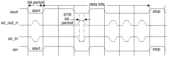
When IrDA SIR mode is enabled, the UART operates in a manner similar to when the mode is disabled, with one exception: data transfers can only occur in half-duplex fashion when IrDA SIR mode is enabled. This is because the IrDA SIR physical layer specifies a minimum of 10 ms delay between transmission and reception; this 10 ms delay must be generated by software.
Registers
RBR
-
Name: Receive Buffer Register
-
Description: This register can be accessed only when the DLAB bit (LCR[7]) is cleared.
-
Base Address: 0x4000C500 + x*0x100
-
Offset: 0x0
-
Reset Value: 0x00000000
*x is used to identify the UART Module instance. The “x” can be 0 or 1.
| Bits | Field Name | RW | Reset | Description |
|---|---|---|---|---|
31:8 |
RSVD |
R |
Reserved bits |
|
7:0 |
RBR |
R |
0x0 |
Receive Buffer Register. This register contains the data byte received on the serial input port (sin) in UART mode. The data in this register is valid only if the Data Ready (DR) bit in the Line Status Register (LSR) is set. |
DLL
-
Name: Divisor Latch Low Register
-
Description: This register can be accessed only when the DLAB bit (LCR[7]) is set.
-
Base Address: 0x4000C500 + x*0x100
-
Offset: 0x00
-
Reset Value: 0x00000000
| Bits | Field Name | RW | Reset | Description |
|---|---|---|---|---|
31:8 |
RSVD |
R |
Reserved bits |
|
7:0 |
DLL |
RW |
0x0 |
Divisor Latch (Low). This register makes up the lower 8 bits of a 16-bit, read/write, Divisor Latch register that contains the baud rate divisor for the UART. Note that with the Divisor Latch Registers (DLL and DLH) set to zero, the baud clock is disabled and no serial communications will occur. In addition, once the DLL is set, at least 8 clock cycles of the slowest UART clock should be allowed to pass before transmitting or receiving data. |
THR
-
Name: Transmit Holding Register
-
Description: This register can be accessed only when the DLAB bit (LCR[7]) is cleared.
-
Base Address: 0x4000C500 + x*0x100
-
Offset: 0x00
-
Reset Value: 0x00000000
| Bits | Field Name | RW | Reset | Description |
|---|---|---|---|---|
31:8 |
RSVD |
R |
0x0 |
Reserved bits |
7:0 |
THR |
W |
0x0 |
Transmit Holding Register. This register contains data to be transmitted on the serial output port (sout) in UART mode. Data should only be written to the TXR when the TXR Empty (THRE) bit (LSR [5]) is set. |
DLH
-
Name: Divisor Latch High Register
-
Description: This register can be accessed only when the DLAB bit (LCR [7]) is set.
-
Base Address: 0x4000C500 + x*0x100
-
Offset: 0x04
-
Reset Value: 0x00000000
| Bits | Field Name | RW | Reset | Description |
|---|---|---|---|---|
31:8 |
RSVD |
R |
Reserved bits |
|
7:0 |
DLH |
RW |
0x0 |
Divisor Latch (HIGH). Upper 8-bit of a 16-bit, read/write, Divisor Latch register that contains the baud rate divisor for the UART. Note that with the Divisor Latch Registers (DLL and DLH) set to zero, the baud clock is disabled and no serial communications will occur. Also, once the DLH is set, at least 8 clock cycles of the slowest UART clock should be allowed to pass before transmitting or receiving data. |
IER
-
Name: Interrupt Enable Register
-
Description: This register can be accessed only when the DLAB bit (LCR [7]) is cleared.
-
Base Address: 0x4000C500 + x*0x100
-
Offset: 0x04
-
Reset Value: 0x00000000
| Bits | Field Name | RW | Reset | Description |
|---|---|---|---|---|
31:8 |
RSVD |
R |
Reserved bits |
|
7 |
PTIME |
RW |
0x0 |
This is used to enable/disable the generation of THRE Interrupt. Value:
|
6:4 |
RSVD |
R |
Reserved bits |
|
3 |
EDSSI |
RW |
0x0 |
Enable Modem Status Interrupt. This is used to enable/disable the generation of Modem Status Interrupt. This is the fourth highest priority interrupt. Value:
|
2 |
ERLS |
RW |
0x0 |
Enable Receiver Line Status Interrupt. This is used to enable/disable the generation of Receiver Line Status Interrupt. This is the highest priority interrupt. Value:
|
1 |
ETBEI |
RW |
0x0 |
Enable Transmit Holding Register Empty Interrupt. This is used to enable/disable the generation of Transmitter Holding Register Empty Interrupt. This is the third highest priority interrupt. Value:
|
0 |
ERBFI |
RW |
0x0 |
Enable Received Data Available Interrupt. This is used to enable/disable the generation of Received Data Available Interrupt and the Character Timeout Interrupt (if in FIFO mode and FIFO's enabled). These are the second highest priority interrupts. Value:
|
FCR
-
Name: FIFO Control Register
-
Description: FIFO Control Register
-
Base Address: 0x4000C500 + x*0x100
-
Offset: 0x08
-
Reset Value: 0x00000400
| Bits | Field Name | RW | Reset | Description |
|---|---|---|---|---|
31:8 |
RSVD |
R |
Reserved bits |
|
7:6 |
RT |
W |
0x0 |
RX Trigger (or RX_FIFO_TRG). This is used to select the trigger level in the receiver FIFO at which the Received Data Available Interrupt will be generated. In auto flow control mode, it is used to determine when the rts_n signal will be de-asserted. It also determines when the dma_rx_req_n signal will be asserted when in certain modes of operation. Value:
|
5:4 |
TET |
W |
0x0 |
TX Empty Trigger (or TX_EMPTY_TRG). This is used to select the empty threshold level at which the THRE Interrupts will be generated when the mode is active. It also determines when the dma_tx_req_n signal will be asserted when in certain modes of operation. Value:
|
3 |
DMA_MODE |
W |
0x0 |
DMA Mode (or DMA_MODE). This determines the DMA signaling mode used for the dma_tx_req_n and dma_rx_req_n output signals when additional DMA handshaking signals are not selected. Value:
|
2 |
XFIFOR |
W |
0x0 |
TX FIFO Reset (or TX_FIFO_RST). This resets the control portion of the transmit FIFO and treats the FIFO as empty. This will also de-assert the DMA TX request and single signals when additional DMA handshaking signals are selected. Value: 0x1 (RESET): Transmit FIFO reset |
1 |
RFIFOR |
W |
0x0 |
RX FIFO Reset (or RX_FIFO_RST). This resets the control portion of the receive FIFO and treats the FIFO as empty. This will also de-assert the DMA RX request and single signals when additional DMA handshaking signals are selected. Value: 0x1 (RESET): Receive FIFO reset |
0 |
FIFOE |
W |
0x0 |
FIFO Enable (or FIFO_EN). This enables/disables the transmit (TX) and receive (RX) FIFOs. Whenever the value of this bit is changed both the TX and RX controller portion of FIFOs is reset. Value:
|
IIR
-
Name: Interrupt Identification Register
-
Description: Interrupt Identification Register
-
Base Address: 0x4000C500 + x*0x100
-
Offset: 0x08
-
Reset Value: 0x00000001
| Bits | Field Name | RW | Reset | Description |
|---|---|---|---|---|
31:8 |
RSVD |
R |
Reserved bits |
|
7:6 |
FIFO_EN |
R |
0x0 |
FIFOs Enabled (or FIFO_EN). This is used to indicate whether the FIFOs are enabled or disabled. Value:
|
5:4 |
RSVD |
R |
Reserved bits |
|
3:0 |
IID |
R |
0x1 |
Interrupt ID (or priority index). This indicates the highest priority pending interrupt which can be one of the following types specified in Values. Value:
|
LCR
-
Name: Line Control Register
-
Description: Line Control Register
-
Base Address: 0x4000C500 + x*0x100
-
Offset: 0x0C
-
Reset Value: 0x00000000
| Bits | Field Name | RW | Reset | Description |
|---|---|---|---|---|
| 31:8 |
RSVD |
R |
Reserved bits |
|
| 7 |
DLAB |
RW |
0x0 |
Divisor Latch Access Bit. This bit is used to enable reading and writing of the Divisor Latch Register (DLL and DLH) to set the baud rate of the UART. This bit must be cleared after initial baud rate setup in order to access other registers. Value:
|
| 6 |
BC |
RW |
0x0 |
Break Control Bit. This is used to cause a break condition to be transmitted to the receiving device. If set to one the serial output is forced to the spacing (logic 0) state. When not in Loopback Mode, as determined by MCR[4], the sout line is forced low until the Break bit is cleared. When in Loopback Mode, the break condition is internally looped back to the receiver and the sir_out_n line is forced low. Value:
|
| 5 |
STICK_PARITY |
RW |
0x0 |
Stick Parity. This bit is used to force parity value. When PARITY, EVEN_PARITY_SEL and STICK_PARITY are set to 1, the parity bit is transmitted and checked as logic 0. If PARITY and Stick Parity are set to 1 and EVEN_PARITY_SEL is a logic 0, then parity bit is transmitted and checked as a logic 1. If this bit is set to 0, Stick Parity is disabled. Value:
|
| 4 |
EVEN_PARITY_SEL |
RW |
0x0 |
Even Parity Select. This is used to select between even and odd parity, when parity is enabled (PEN set to one). If this bit is set to one, an even number of logic '1's is transmitted or checked. If set to zero, an odd number of logic '1's is transmitted or checked. Value:
|
| 3 |
PARITY |
RW |
0x0 |
Parity Enable. This bit is used to enable and disable parity generation and detection in transmitted and received serial character respectively. Value:
|
| 2 |
STOP |
RW |
0x0 |
Number of Stop bits. This is used to select the number of Stop bits per character that the peripheral will transmit and receive. If set to zero, one stop bit is transmitted in the serial data. If this bit is set to one and the Data bits are set to 5 (LCR[1:0] set to zero), one and a half Stop bits are transmitted. Otherwise, two Stop bits are transmitted. Note that regardless of the number of stop bits selected, the receiver will only check the first Stop bit. Note: The Stop bit duration implemented by UART may appear longer due to idle time inserted between characters for some configurations and baud clock divisor values in the transmit direction. Value:
|
| 1:0 |
DLS |
RW |
0x0 |
Data Length Select (or CLS as used in legacy). Wthis register is used to select the number of data bits per character that the peripheral will transmit and receive. Value:
|
MCR
-
Name: Modem Control Register
-
Description: Modem Control Register
-
Base Address: 0x4000C500 + x*0x100
-
Offset: 0x10
-
Reset Value: 0x00000000
| Bits | Field Name | RW | Reset | Description |
|---|---|---|---|---|
31:6 |
RSVD |
R |
Reserved bits |
|
5 |
AFCE |
RW |
0x0 |
Auto Flow Control Enable When FIFOs are enabled and the Auto Flow Control Enable (AFCE) bit is set, Auto Flow Control features are enabled as described in “Auto Flow Control”. Value:
|
4 |
LOOPBACK |
RW |
0x0 |
Loopback Bit. This is used to put the UART into a diagnostic mode for test purposes. Value:
|
3:2 |
RSVD |
R |
Reserved bits |
|
1 |
RTS |
RW |
0x0 |
Request to Send. This is used to directly control the Request to Send (rts_n) output. The Request To Send (rts_n) output is used to inform the modem or data set that the UART is ready to exchange data. Value:
|
0 |
RSVD |
R |
Reserved bits |
LSR
-
Name: Line Status Register
-
Description: Line Status Register
-
Base Address: 0x4000C500 + x*0x100
-
Offset: 0x14
-
Reset Value: 0x00000000
| Bits | Field Name | RW | Reset | Description |
|---|---|---|---|---|
31:8 |
RSVD |
R |
Reserved bits |
|
7 |
RFE |
R |
0x0 |
Receiver FIFO Error bit. This is used to indicate if there is at least one parity error, framing error, or break indication in the FIFO. This bit is cleared when the LSR is read and the character with the error is at the top of the receiver FIFO and there are no subsequent errors in the FIFO. Value:
|
6 |
TEMT |
R |
0x1 |
Transmitter Empty bit. If FIFO is enabled (FCR[0] set to one), this bit is set whenever the Transmitter Shift Register and the FIFO are both empty. Value:
|
5 |
THRE |
R |
0x1 |
Transmit Holding Register Empty bit. If THRE mode is disabled (IER[7] set to zero) and regardless of FIFO's being implemented/enabled or not, this bit indicates that the THR or TX FIFO is empty. Value:
|
4 |
BI |
R |
0x0 |
Break Interrupt bit. This is used to indicate the detection of a break sequence on the serial input data. Value:
|
3 |
FE |
R |
0x0 |
Framing Error bit. This is used to indicate the occurrence of a framing error in the receiver. A framing error occurs when the receiver does not detect a valid STOP bit in the received data. Value:
|
2 |
PE |
R |
0x0 |
Parity Error bit. This is used to indicate the occurrence of a parity error in the receiver if the Parity Enable (PARITY) bit (LCR[3]) is set. Value:
|
1 |
OE |
R |
0x0 |
Overrun error bit. This is used to indicate the occurrence of an overrun error. This occurs if a new data character was received before the previous data was read. Value:
|
0 |
DR |
R |
0x0 |
Data Ready bit. This is used to indicate that the receiver contains at least one character in the RBR or the receiver FIFO. This bit is cleared when the receiver FIFO is empty, in the FIFO mode. Value:
|
MSR
-
Name: Modem Status Register
-
Description: Whenever bit 0 is set to logic 1 to indicate a change on the modem control inputs, a modem status interrupt will be generated if enabled via the INT_EN regardless of when the change occurred. The bits (bit 0) can be set after a reset, even though their respective modem signals are inactive, because the synchronized version of the modem signals have a reset value of 0 and change to value 1 after reset. To prevent unwanted interrupts due to this change, a read of the MSR register can be performed after reset.
-
Base Address: 0x4000C500 + x*0x100
-
Offset: 0x18
-
Reset Value: 0x00000000
| Bits | Field Name | RW | Reset | Description |
|---|---|---|---|---|
31:5 |
RSVD |
R |
Reserved bits |
|
4 |
CTS |
R |
0x0 |
Clear to Send. This is used to indicate the current state of the modem control line cts_n. That is, this bit is the complement cts_n. When the Clear to Send input (cts_n) is asserted, it is an indication that the modem or data set is ready to exchange data with the UART. In Loopback Mode (MCR[4] set to one), CLR_SEND is the same as MCR[1] (RTS). Value:
|
3:1 |
RSVD |
R |
Reserved bits |
|
0 |
DCTS |
R |
0x0 |
Delta Clear to Send. This is used to indicate that the modem control line cts_n has changed since the last time the MSR was read. Reading the MSR clears the DCTS bit. In Loopback Mode (MCR[4] set to one), DCTS reflects changes on MCR[1] (RTS). Note: If the DCTS bit is not set and the cts_n signal is asserted (low) and a reset occurs (software or otherwise), then the DCTS bit will get set when the reset is removed if the cts_n signal remains asserted. Value:
|
SRBR
-
Name: Shadow Receive Buffer Register
-
Description: This register can be accessed only when the DLAB bit (LCR[7]) is cleared.
-
Base Address: 0x4000C500 + x*0x100
-
Offset: 0x30
-
Reset Value: 0x00000000
| Bits | Field Name | RW | Reset | Description |
|---|---|---|---|---|
31:8 |
RSVD |
R |
Reserved bits |
|
7:0 |
SHADOW_RX_BUFn |
R |
Shadow Receive Buffer Register n. This is a shadow register for the RBR and has been allocated sixteen 32-bit locations so as to accommodate burst accesses from the master. This register contains the data byte received on the serial input port (sin) in UART mode. The data in this register is valid only if the Data Ready (DR) bit in the Line Status Register (LSR) is set.
|
STHR
-
Name: Shadow Transmit Holding Register
-
Description: This register can be accessed only when the DLAB bit (LCR[7]) is cleared.
-
Base Address: 0x4000C500 + x*0x100
-
Offset: 0x30
-
Reset Value: 0x00000000
| Bits | Field Name | RW | Reset | Description |
|---|---|---|---|---|
31:8 |
RSVD_STHRn |
R |
SHADOW_TX_HDG0 31 to SHADOW_TX_HDGN_REG_SIZE Reserved bits read as 0. |
|
7:0 |
SHADOW_TX_HDGn |
W |
0x0 |
Shadow Transmit Holding Register n. This is a shadow register for the THR and has been allocated sixteen 32-bit locations so as to accommodate burst accesses from the master. This register contains data to be transmitted on the serial output port (sout) in UART mode. Data should only be written to the THR when the THR Empty (THRE) bit (LSR[5]) is set.
|
FAR
-
Name: FIFO Access Register
-
Description: FIFO Access Register
-
Base Address: 0x4000C500 + x*0x100
-
Offset: 0x70
-
Reset Value: 0x00000000
| Bits | Field Name | RW | Reset | Description |
|---|---|---|---|---|
31:1 |
RSVD |
R |
Reserved bits |
|
0 |
FIFO_ACCESS |
R |
0x0 |
This register is use to enable a FIFO access mode for testing, so that the receive FIFO can be written by the master and the transmit FIFO can be read by the master when FIFO's are implemented and enabled. When FIFOs are not implemented or not enabled, it allows the RBR to be written by the master and the THR to be read by the master. Note: When the FIFO access mode is enabled/disabled, the control portion of the receive FIFO and transmit FIFO is reset and the FIFO's are treated as empty. Value:
|
USR
-
Name: UART Status Register
-
Description: UART Status register
-
Base Address: 0x4000C500 + x*0x100
-
Offset: 0x7C
-
Reset Value: 0x00000000
| Bits | Field Name | RW | Reset | Description |
|---|---|---|---|---|
31:5 |
RSVD |
R |
Reserved bits |
|
4 |
RFF |
R |
0x0 |
Receive FIFO Full. This is used to indicate that the receive FIFO is completely full. This bit is cleared when the RX FIFO is no longer full. Value:
|
3 |
RFNE |
R |
0x0 |
Receive FIFO Not Empty. This is used to indicate that the receive FIFO contains one or more entries. This bit is cleared when the RX FIFO is empty. Value:
|
2 |
TFE |
R |
0x1 |
Transmit FIFO Empty. This is used to indicate that the transmit FIFO is completely empty. This bit is cleared when the TX FIFO is no longer empty. Value:
|
1 |
TFNF |
R |
0x1 |
Transmit FIFO Not Full. This is used to indicate that the transmit FIFO in not full. This bit is cleared when the TX FIFO is full. Value:
|
0 |
RSVD |
R |
Reserved bit |
TFL
-
Name: Transmit FIFO Level
-
Description: Transmit FIFO Level
-
Base Address: 0x4000C500 + x*0x100
-
Offset: 0x80
-
Reset Value: 0x00000000
| Bits | Field Name | RW | Reset | Description |
|---|---|---|---|---|
31:8 |
RSVD |
R |
Reserved bits |
|
7:0 |
TFL |
R |
0x0 |
Transmit FIFO Level. This indicates the number of data entries in the transmit FIFO. |
RFL
-
Name: Receive FIFO Level
-
Description: Receive FIFO Level
-
Base Address: 0x4000C500 + x*0x100
-
Offset: 0x84
-
Reset Value: 0x00000000
| Bits | Field Name | RW | Reset | Description |
|---|---|---|---|---|
31:8 |
RSVD |
R |
Reserved bits |
|
7:0 |
RFL |
R |
0x0 |
Receive FIFO Level. This is indicates the number of data entries in the receive FIFO. |
SRR
-
Name: Software Reset Register
-
Description: Software Reset Register
-
Base Address: 0x4000C500 + x*0x100
-
Offset: 0x88
-
Reset Value: 0x00000000
| Bits | Field Name | RW | Reset | Description |
|---|---|---|---|---|
| 31:3 |
RSVD |
R |
Reserved bits |
|
| 2 |
XFR |
W |
0x0 |
TX FIFO Reset. This is a shadow register for the TX FIFO Reset bit (FCR[2]). This can be used to remove the burden on software having to store previously written FCR values (which are pretty static) just to reset the transmit FIFO |
| 1 |
RFR |
W |
0x0 |
RX FIFO Reset. This is a shadow register for the RX FIFO Reset bit (FCR[1]). This can be used to remove the burden on software having to store previously written FCR values (which are pretty static) just to reset the receive FIFO. |
| 0 |
UR |
W |
0x0 |
UART Reset. This asynchronously resets the UART and synchronously removes the reset assertion. For a two-clock implementation both PCLK and SCLK domains will be reset. Value:
|
SRTS
-
Name: Shadow Request to Send Register
-
Description: Shadow Request to Send
-
Base Address: 0x4000C500 + x*0x100
-
Offset: 0x8C
-
Reset Value: 0x00000000
| Bits | Field Name | RW | Reset | Description |
|---|---|---|---|---|
31:1 |
RSVD |
R |
Reserved bits |
|
0 |
SRTS |
RW |
0x0 |
Shadow Request to Send. This is a shadow register for the RTS bit (MCR [1]), this can be used to remove the burden of having to performing a read modify write on the MCR. This is used to directly control the Request to Send (rts_n) output. The Request To Send (rts_n) output is used to inform the modem or data set that the UART is ready to exchange data. Value:
|
SBCR
-
Name: Shadow Break Control Register
-
Description: Shadow Break Control Register
-
Base Address: 0x4000C500 + x*0x100
-
Offset: 0x90
-
Reset Value: 0x00000000
| Bits | Field Name | RW | Reset | Description |
|---|---|---|---|---|
31:1 |
RSVD |
R |
Reserved bits |
|
0 |
SBCR |
RW |
0x0 |
Shadow Break Control Bit. This is a shadow register for the Break bit (LCR[6]). This can be used to remove the burden of having to performing a read modify write on the LCR. This is used to cause a break condition to be transmitted to the receiving device. If set to one the serial output is forced to the spacing (logic 0) state. When not in Loopback Mode, as determined by MCR [4], the sout line is forced to be low until the Break bit is cleared. Value:
|
SFE
-
Name: Shadow FIFO Enable Register
-
Description: Shadow FIFO Enable Register
-
Base Address: 0x4000C500 + x*0x100
-
Offset: 0x98
-
Reset Value: 0x00000000
| Bits | Field Name | RW | Reset | Description |
|---|---|---|---|---|
31:1 |
RSVD |
R |
Reserved bits |
|
0 |
SFE |
RW |
0x0 |
Shadow FIFO Enable. This is a shadow register for the FIFO enable bit (FCR[0]). This can be used to remove the burden of having to store the previously written value to the FCR in memory and having to mask this value so that only the FIFO enable bit gets updated. This enables/disables the transmit (TX) and receive (RX) FIFO's. If this bit is set to zero (disabled) after being enabled then both the TX and RX controller portions of FIFO's will be reset. Value:
|
SRT
-
Name: Shadow RX Trigger Register
-
Description: Shadow RX Trigger Register
-
Base Address: 0x4000C500 + x*0x100
-
Offset: 0x9C
-
Reset Value: 0x00000000
| Bits | Field Name | RW | Reset | Description |
|---|---|---|---|---|
31:2 |
RSVD |
R |
Reserved bits |
|
1:0 |
SRT |
RW |
0x0 |
Shadow RX Trigger. This is a shadow register for the RX trigger bits (FCR[7:6]). This can be used to remove the burden of having to store the previously written value to the FCR in memory and having to mask this value so that only the RX trigger bit gets updated. Value:
|
STET
-
Name: Shadow TX Empty Trigger Register
-
Description: Shadow TX Empty Trigger Register
-
Base Address: 0x4000C500 + x*0x100
-
Offset: 0xA0
-
Reset Value: 0x00000000
| Bits | Field Name | RW | Reset | Description |
|---|---|---|---|---|
31:2 |
RSVD |
R |
Reserved bits |
|
1:0 |
STET |
RW |
0x0 |
Shadow TX Empty Trigger. This is a shadow register for the TX empty trigger bits (FCR[5:4]). This can be used to remove the burden of having to store the previously written value to the FCR in memory and having to mask this value so that only the TX empty trigger bit gets updated. Value:
|
HTX
-
Name: Halt TX Register
-
Description: Halt TX
-
Base Address: 0x4000C500 + x*0x100
-
Offset: 0xA4
-
Reset Value: 0x00000000
| Bits | Field Name | RW | Reset | Description |
|---|---|---|---|---|
31:1 |
RSVD |
R |
Reserved bits |
|
0 |
HTX |
RW |
0x0 |
Halt TX. This register is use to halt transmissions for testing, so that the transmit FIFO can be filled by the master when FIFOs are implemented and enabled. Value:
|
DLF
-
Name: Divisor Latch Fraction Register
-
Description: Divisor Latch Fraction Register
-
Base Address: 0x4000C500 + x*0x100
-
Offset: 0xC0
-
Reset Value: 0x00000000
| Bits | Field Name | RW | Reset | Description |
|---|---|---|---|---|
31:4 |
RSVD |
R |
Reserved bits |
|
3:0 |
DLF |
RW |
0x0 |
Fractional part of divisor. The fractional value is added to integer value set by DLH and DLL. Fractional value is determined by (Divisor Fraction value, DLF.DLF)/(2^DLF_SIZE), where DLF_SIZE = 4. |
Electrical Specifications
| Baud Rate | Divider | DLH Reg | DLL Reg | DLF Reg | Actual Baud Rate | Error (%) |
|---|---|---|---|---|---|---|
| 1200 | 3333.33 | 13 | 5 | 5 | 1200 | 0 |
| 2400 | 1666.67 | 6 | 130 | 11 | 2399.97 | 0 |
| 4800 | 833.33 | 3 | 65 | 5 | 4800.12 | 0 |
| 9600 | 416.67 | 1 | 160 | 11 | 9599.52 | 0.05 |
| 14400 | 277.78 | 1 | 21 | 12 | 14401.44 | 0.01 |
| 19200 | 208.33 | 0 | 208 | 6 | 19201.92 | 0.01 |
| 28800 | 138.89 | 0 | 138 | 14 | 28802.88 | 0.01 |
| 38400 | 104.17 | 0 | 104 | 3 | 38392.32 | 0.02 |
| 57600 | 69.44 | 0 | 69 | 7 | 57605.76 | 0.01 |
| 115200 | 34.72 | 0 | 34 | 12 | 115107.91 | 0.08 |
| 230400 | 17.36 | 0 | 17 | 6 | 230215.83 | 0.08 |
| 460800 | 8.68 | 0 | 8 | 11 | 460431.65 | 0.08 |
| 921600 | 4.34 | 0 | 4 | 5 | 927536.23 | 0.64 |
| 1000000 | 4 | 0 | 4 | 0 | 1000000 | 0 |
| 2000000 | 2 | 0 | 2 | 0 | 2000000 | 0 |
