
PWM
Introduction
The device has two instances of Pulse Width Modulation (PWM) module. The PWM generates successive pulses with variable duty cycles that can be converted to analog levels by external discrete components, such as controlling LED brightness via a PWM signal. One of the PWM instance supports coding mode in order to drive LED control unit conveniently.
Main Features
- Configurable output frequency and dynamic frequency configuration
- Three independent PWM channel outputs for each instance: pwma, pwmb, and pwmc
- Three operation modes: flicker mode, breath mode and coding mode.
- Two alignment modes: edge aligned mode and center aligned mode
- Configurable duty cycles in flicker mode
- Customizable number of PWM cycles
- DMA supported in coding mode
- An independent interrupt entry in coding mode
- Three configuration modes: synchronize-all, synchronize-separate, and asynchronous
- Polarity switching to support positive-drive and negative-drive mode
- Optional stop I/O voltage level in active/idle mode: low level or high level
Block Diagram
The PWM block diagram is illustrated in the figure below.

Functional Description
The PWM module has two instances which are PWM0 and PWM1. There are three operation modes: flicker mode, breath mode and coding mode. Only PWM0 instance supports the coding mode. Each PWM instance can provide three independent channel outputs: pwma, pwmb and pwmc. Each channel shares the same frequency, but can be configured with different duty cycles.
- In positive-drive mode, a valid output is configured by setting the PWM output logic level to 1, whereas an invalid output is set when the PWM output logic level is 0.
- In negative-drive mode, a valid output is configured by setting the PWM output logic level to 0, whereas an invalid output is set when PWM output logic level is 1.
The PWM module supports customizable number of PWM cycles. PRD_CYCLES register can control the number of cycles. This function is only valid when the PRD_CYCLES value is greater than 0.
Flicker Mode
In flicker mode, the PWM module outputs successive pulses with a certain frequency and duty as configured. The PRD register is used to configure the frequency in flicker mode. The duty of PWM can be configured in the range of 0% to 100% through the CMPx0, CMPx1, and AQCTRL registers. The three outputs can be configured independently, and they share the same output frequency.

In flicker mode, if the stop level is configured (the default value of FLICKER_PAUSE_LEVEL_x is 0 when not set), the I/O level of the corresponding channel will be pulled to the set value when PWM stops.
Breath Mode
In breath mode, the duty of PWM output periodically changes from 0% to 100%, and then 100% to 0% uniformly. The breathing cycle can be set by the BRPRD register, which represents the number of PWM cycles required for the duty cycle 0%→100% and then 100%→0%.
A configurable duration of breath hold state (can be set by the HOLD rgister) is supported. The breath hold state is set between two adjacent breath processes, that is duty change (0%→100%→0%), breath hold, and duty change (0%→100%→0%). In the hold state, the PWM output is driven by inactive state.
In breath mode, the I/O levels of all channels are the same and set by the BREATH_PAUSE_LEVEL bit in the MODE register when PWM stops. When the MCU enters sleep state, the stop level remains high in both flicker mode and breath mode.
Coding Mode
The PWM0 instance supports coding mode. In coding mode, the PWM waveform is determined by the coded data. The coding mode supports single-channel output and three-channel output. Each channel shares the same frequency but can be coded with different data.
The duty cycle of code “0” and code “1” can be configured through the CMPx0, CMPx1, and AQCTRL registers. Write the encoded data to the CODING_DATA register in order to output the specified PWM waveform. The CODING_DATA register will only take effect when MODE.CODINGEN is enabled. The valid bit width of CODING_DATA register is controlled by DATA_WIDTH_VALID register. The default configuration is 32-bit valid bit width and all channels are shared with the DATA_WIDTH_VALID register. Through the coordination of DATA_WIDTH_VALID register and PRD_CYCLES register, the specified number of encoded PWM waveforms can be controlled.
The WAIT_TIME register can control the wait time before start coding. All channels are shared the WAIT_TIME register. The function of configuring wait time can be enabled through the field WAITING_TIME_LEVEL_x in the MODE register.
The coded data flow supports MCU control and DMA control.
- In MCU control mode, it is necessary to write coding data to the CODING_DATA register to control the PWM waveform.
- In single-channel mode, it is only necessary to write the coding data to the CODING_DATA register once.
- In three-channel mode, it is necessary to write three consecutive coding data to the CODING_DATA register. The encoded data written sequentially will take effect on different channels in sequence.
- In DMA control mode, the PWM module supports configure the coded data from RAM to CODING_DATA register through DMA.
- In single-channel mode, the DMA burst length is 1-word, which is used to transfer the data of 1-word to CODING_DATA register.
- In three-channel mode, the DMA burst length is 4-word, which is used to transfer the data of 3-word to CODING_DATA register. The three channels will be encoded respectively, while the last word data is discarded. Therefore, the burst length of DMA should be an integer multiple of 4 in three-channel mode.

In coding mode, when the coded data required by the PWM controller is too late to be written into the CODING_DATA register, a coding error interrupt will be generated. The coding status of the 3 channels can be checked through the CODING_STATUS[2:0] bits. If the encoded data is not written when the PWM controller reads, the CODING_x_ERROR bit of the specified channel will be set to 1. When the encoding is completed, a completion interrupt will be generated, the CODING_STATUS[3] bit will be set to 1. In MCU control mode, the CODING_STATUS[4] bit can be used to determine whether to write coded data.
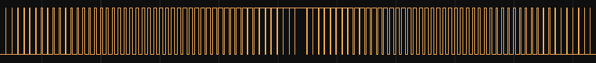
Generating Encoded Waveforms
For example, the encoded PWM waveforms are shown in 图 47.
- PWM frequency is 1000 clocks.
- Negative-drive mode
- PWMA channel: code "1" as 300 clocks, code "0" as 800 clocks
- PWMB channel: code "1" as 400 clocks, code "0" as 700 clocks
- PWMC channel: code "1" as 200 clocks, code "0" as 900 clocks
- Coding wait time is 5000 clocks.
- The level of PWMA is high level during the wait time, and the levels of PWMB and PWMC are low level during the wait time.
- PWM output cycle number is 16.
- Valid Data Width is 0xF.
- PWMA/PWMB/PWMC coding data is 0x0569/0x016d/0x8051.

PWMC' is the output waveforms when PWMC is configured with opposite polarity.
Generating Waveforms with Arbitrary Duty Cycles
The coding mode can be used to control the output of PWM waveforms with different duty cycle and period so as to achieve the lighting control requirements.
Take single channel in coding mode as an example. Configure the PWM period as 1000 clocks, the duty cycle of code “0” as 1000 clocks and the duty cycle of code “1” as 0 clock. Through the coding sequence "1000_1100_1110", three PWM pulses with duty cycles of 25%, 50%, 75% and 4000 clocks period can be generated.

Alignment
In flicker mode, both edge-aligned and center-aligned modes are supported through software approach.
-
Choose edge-aligned mode, as shown in the figure below. All open channels are aligned at the beginning of each duty cycle.

图 49 PWM edge alignment -
Choose center-aligned mode, as shown in the following figure. All open channels are aligned in the middle of each duty cycle.

图 50 PWM center alignment
Active Update
PWM module is capable of configuring output frequency dynamically. There are several shadow registers in the PWM module. The write operation will first change the shadow registers, and then will update the value of active registers from the shadow registers under certain conditions.
The configured data can be updated into active registers in three modes: synchronize-all mode (enabled by UPDATE.SA), synchronize-separate mode (enabled by UPDATE.SSCMPxx) and asynchronous update mode (enabled by UPDATE.SA and UPDATE. SSCMPxx).
Active registers update conditions:
-
In synchronize-all update mode (UPDATE.SA = 0x1), all effective registers of flicker mode or breath mode will be updated simultaneously. In flicker mode (MODE.BREATHEN = 0), after writing to PRD, the CMPxx and AQCTRL registers will update from the shadow registers simultaneously when the Time Base counter counts to a value of PRD minus 1.
In breath mode ((MODE.BREATHEN = 1), after writing to PRD, the BRPRD and HOLD registers will update from shadow registers simultaneously when the current breath process ends (the moment PWM duty reduces to 0%). When using the app_pwm_update_freq interface, the PWM frequency will be updated immediately.
-
In synchronize-separate update mode (UPDATE.SA = 0x0), the PRD, CMPxx, and AQCTRL registers will update when the Time Base counter counts to value of the PRD register minus 1, and if the corresponding UPDATE.SSCMPxx bit is set. The BRPRD and HOLD registers will update when the current breath process ends and the corresponding UPDATE.SSCMPxx bit is set.
-
In asynchronous update mode (UPDATE.SA = 0x0 and UPDATE.SSCMPxx = 0x0), all registers will update instantly.
If the configurations need to be changed under synchronize-all update mode, the CMPXX and AQCTRL registers in flicker mode, or the HOLD register in breath mode should be written before modifying the values of PRD and BRPRD.
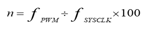
Duty Cycle Calculation
The PWM duty cycle can be configured as an integer from 0 to 100, depending on the following calculation formulas of the duty cycle accuracy "n".
- In edge-aligned mode:
- In center-aligned mode:
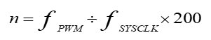
For example, when the clock frequency is 64 MHz, and the duty cycle is in the range of 0 to 100, the maximum PWM frequency can only be set to 640 kHz in the edge-aligned mode and 320 kHz in the center-aligned mode.
Recommended Setting in Breath Mode
In breath mode, in order to ensure that the duty cycle of the waveform changes from 0 to 100 and then from 100 to 0, it is necessary to set the values of PRD and BRPRD to an integer that is multiple(s) of 128. The freq, bperiod. and hperiod in the structure pwm_init_t need to meet the following formula during initialization:
where, k represents the number of PWM cycles required for the duty cycle from 0% to 100%; SYSCLK represents the system clock frequency; bperiod represents the breath period; hperiod represents the hold period.
Registers
PWM0
MODE
- Name: Mode Register
- Description: This register sets the PWM operation mode.
- Base Address: 0x4000CB00
- Offset: 0x0
- Reset Value: 0x00000038
| Bits | Field Name | RW | Reset | Description |
|---|---|---|---|---|
31:16 |
RSVD |
R |
Reserved bits |
|
15 |
CODING_CHANNEL_SELECT |
RW |
0x0 |
Select PWMA/B/C coding channel.
|
14 |
DMA_EN |
RW |
0x0 |
PWMA/B/C coding mode enable DMA
|
13 |
WAITING_TIME_LEVEL_C |
RW |
0x0 |
PWMC waiting time level in coding mode
|
12 |
WAITING_TIME_LEVEL_B |
RW |
0x0 |
PWMB waiting time level in coding mode
|
11 |
WAITING_TIME_LEVEL_A |
RW |
0x0 |
PWMA waiting time level in coding mode
|
10 |
CODINGEN |
RW |
0x0 |
Enable PWMA/B/C coding mode. Value:
|
9 |
BREATH_PAUSE_LEVEL |
RW |
0x0 |
PWMA/B/C output IO level when suspending in Breath Mode |
8 |
FLIKCER_PAUSE_LEVEL_C |
RW |
0x0 |
PWMC output IO level when suspending in Flicker Mode |
7 |
FLIKCER_PAUSE_LEVEL_B |
RW |
0x0 |
PWMB output IO level when suspending in Flicker Mode |
6 |
FLIKCER_PAUSE_LEVEL_A |
RW |
0x0 |
PWMA output IO level when suspending in Flicker Mode |
5 |
DPENC |
RW |
0x1 |
Enable PWMC positive-drive mode. Value:
|
4 |
DPENB |
RW |
0x1 |
Enable PWMB positive-drive mode. Value:
|
3 |
DPENA |
RW |
0x1 |
Enable PWMA positive-drive mode. Value:
|
2 |
BREATHEN |
RW |
0x0 |
Enable Breath mode. Value:
|
1 |
PAUSE |
RW |
0x0 |
PWM pause signal Value:
|
0 |
EN |
RW |
0x0 |
Enable PWM. Value:
|
UPDATE
- Name: Update Register
- Description: This register is used to set the synchronous update mode.
- Base Address: 0x4000CB00
- Offset: 0x4
- Reset Value: 0x00000000
| Bits | Field Name | RW | Reset | Description |
|---|---|---|---|---|
| 31:18 | RSVD | R | Reserved bits | |
| 17 | SSAQCTRL | RW | 0x0 | Enable separate update of AQCTRL Value:
|
| 16 | SSHOLD | RW | 0x0 | Enable separate update of HOLD Value:
|
| 15 | SSBRPRD | RW | 0x0 | Enable separate update of BRPRD Value:
|
| 14 | SSCMPC1 | RW | 0x0 | Enable separate update of CMPC1 Value:
|
| 13 | SSCMPC0 | RW | 0x0 | Enable separate update of CMPC0 Value:
|
| 12 | SSCMPB1 | RW | 0x0 | Enable separate update of CMPB1 Value:
|
| 11 | SSCMPB0 | RW | 0x0 | Enable separate update of CMPB0 Value:
|
| 10 | SSCMPA1 | RW | 0x0 | Enable separate update of CMPA1 Value:
|
| 9 | SSCMPA0 | RW | 0x0 | Enable separate update of CMPA0 Value:
|
| 8 | SSPRD | RW | 0x0 | Enable separate update of PRD Value:
|
| 7:2 | RSVD | R | Reserved bits | |
| 1 | SA | RW | 0x0 | Enable synchronous update Value:
|
| 0 | SAG | R | 0x0 | Synchronous update ongoing Value:
|
PRD
- Name: Period Register
- Description: This register is used to set the PWM cycle.
- Base Address: 0x4000CB00
- Offset: 0x8
- Reset Value: 0x64
| Bits | Field Name | RW | Reset | Description |
|---|---|---|---|---|
31:0 |
PRD |
RW |
0x64 |
The period of PWM output, PRD=fCLK/fPWM |
CMPA0
- Name: Compare A0 Register
- Description: This register controls the PWM duty of Compare register 0 of channel A.
- Base Address: 0x4000CB00
- Offset: 0xC
- Reset Value: 0x00000000
| Bits | Field Name | RW | Reset | Description |
|---|---|---|---|---|
31:0 |
CMPA0 |
RW |
0x0 |
PWMA duty control register0 |
CMPA1
- Name: Compare A1 Register
- Description: This register controls the PWM duty of Compare register 1 of channel A.
- Base Address: 0x4000CB00
- Offset: 0x10
- Reset Value: 0x00000000
| Bits | Field Name | RW | Reset | Description |
|---|---|---|---|---|
31:0 |
CMPA1 |
RW |
0x0 |
PWMA duty control register1 |
CMPB0
- Name: Compare B0 Register
- Description: This register controls the PWM duty of Compare register 0 of channel B.
- Base Address: 0x4000CB00
- Offset: 0x14
- Reset Value: 0x00000000
| Bits | Field Name | RW | Reset | Description |
|---|---|---|---|---|
31:0 |
CMPB0 |
RW |
0x0 |
PWMB duty control register0 |
CMPB1
- Name: Compare B1 Register
- Description: This register controls the PWM duty of Compare register 1 of channel B.
- Base Address: 0x4000CB00
- Offset: 0x18
- Reset Value: 0x00000000
| Bits | Field Name | RW | Reset | Description |
|---|---|---|---|---|
31:0 |
CMPB1 |
RW |
0x0 |
PWMB duty control register1 |
CMPC0
- Name: Compare C0 Register
- Description: This register controls the PWM duty of Compare register 0 of channel C.
- Base Address: 0x4000CB00
- Offset: 0x1C
- Reset Value: 0x00000000
| Bits | Field Name | RW | Reset | Description |
|---|---|---|---|---|
31:0 |
CMPC0 |
RW |
0x0 |
PWMC duty control register0 |
CMPC1
- Name: Compare C1 Register
- Description: This register controls the PWM duty of Compare register 1 of channel C.
- Base Address: 0x4000CB00
- Offset: 0x20
- Reset Value: 0x00000000
| Bits | Field Name | RW | Reset | Description |
|---|---|---|---|---|
31:0 |
CMPC1 |
RW |
0x0 |
PWMC duty control register1 |
AQCTRL
- Name: Action Qualifier Control Register
- Description: This register is used to set actions when counter reaches the compare value.
- Base Address: 0x4000CB00
- Offset: 0x24
- Reset Value: 0x00000000
| Bits | Field Name | RW | Reset | Description |
|---|---|---|---|---|
31:12 |
RSVD |
R |
Reserved bits |
|
11:10 |
C1 |
RW |
0x0 |
Action of event CNT_CMPC1 control register Value:
|
9:8 |
C0 |
RW |
0x0 |
Action of event CNT_CMPC0 control register Value:
|
7:6 |
B1 |
RW |
0x0 |
Action of event CNT_CMPB1 control register Value:
|
5:4 |
B0 |
RW |
0x0 |
Action of event CNT_CMPB0 control register Value:
|
3:2 |
A1 |
RW |
0x0 |
Action of event CNT_CMPA1 control register Value:
|
1:0 |
A0 |
RW |
0x0 |
Action of event CNT_CMPA0 control register Value:
|
BRPRD
- Name: Breath Period Register
- Description: This register configures the period of breath mode.
- Base Address: 0x4000CB00
- Offset: 0x28
- Reset Value: 0x00000000
| Bits | Field Name | RW | Reset | Description |
|---|---|---|---|---|
31:0 |
BRPRD |
RW |
0x0 |
Register for breath period that is the required time (number of clock) that the duty changes from 0% to 100% in breath mode. |
HOLD
- Name: Hold Register
- Description: This register configures the hold period in breath mode.
- Base Address: 0x4000CB00
- Offset: 0x2C
- Reset Value: 0x00000000
| Bits | Field Name | RW | Reset | Description |
|---|---|---|---|---|
31:24 |
RSVD |
R |
Reserved bits |
|
23:0 |
HOLD |
RW |
0x0 |
Breath hold control register. The value should be the required number of clock in breath hold state. |
PRD_CYCLES
- Name: Period Cycles Register
- Description: This register configures the numbers of the period cycles.
- Base Address: 0x4000CB00
- Offset: 0x30
- Reset Value: 0x00000000
| Bits | Field Name | RW | Reset | Description |
|---|---|---|---|---|
31:0 |
PRD_CYCLES |
RW |
0x0 |
Control the number of cycles. The value greater than 0 is valid. |
WAIT_TIME
- Name: Wait Time Register
- Description: This register configures PWM waiting time in PWM coding mode.
- Base Address: 0x4000CB00
- Offset: 0x34
- Reset Value: 0x00000000
| Bits | Field Name | RW | Reset | Description |
|---|---|---|---|---|
31:0 |
WAIT_TIME |
RW |
0x0 |
Control PWM waiting time in the coding mode. |
DATA_WIDTH_VALID
- Name: Data Width Valid Register
- Description: This register configures valid data width in PWM coding mode.
- Base Address: 0x4000CB00
- Offset: 0x38
- Reset Value: 0x0000001F
| Bits | Field Name | RW | Reset | Description |
|---|---|---|---|---|
31:5 |
RSVD |
R |
Reserved bits |
|
4:0 |
DATA_WIDTH_VALID |
RW |
0x1F |
Data valid width is (DATA_WIDTH_VALID + 1) |
CODING_DATA
- Name: Coding Data Register
- Description: This register is used to load coding data in PWM coding mode.
- Base Address: 0x4000CB00
- Offset: 0x3C
- Reset Value: 0x00000000
| Bits | Field Name | RW | Reset | Description |
|---|---|---|---|---|
31:0 |
CODING_DATA |
RW |
0x0 |
Coding Data |
CODING_STATUS
- Name: Coding Status Register
- Description: This register indicates the interrupt status in PWM coding mode.
- Base Address: 0x4000CB00
- Offset: 0x40
- Reset Value: 0x00000000
| Bits | Field Name | RW | Reset | Description |
|---|---|---|---|---|
31:5 |
RSVD |
R |
Reserved bits |
|
4 |
CODING_LOAD |
R |
0x0 |
PWM coding load interrupt status. |
3 |
CODING_DONE |
R |
0x0 |
PWM coding done interrupt status. |
2 |
CODING_C_ERROR |
R |
0x0 |
PWMC coding error status. |
1 |
CODING_B_ERROR |
R |
0x0 |
PWMB coding error status. |
0 |
CODING_A_ERROR |
R |
0x0 |
PWMA coding error status. |
CLR_CODING_STATUS
- Name: Coding Status Clear Register
- Description: This register is used to clear the interrupt status in PWM coding mode.
- Base Address: 0x4000CB00
- Offset: 0x44
- Reset Value: 0x00000000
| Bits | Field Name | RW | Reset | Description |
|---|---|---|---|---|
31:5 |
RSVD |
R |
Reserved bits |
|
4 |
CODING_LOAD_CLR |
W |
0x0 |
Clear PWM coding load interrupt status. |
3 |
CODING_DONE_CLR |
W |
0x0 |
Clear PWM coding done interrupt status. |
2 |
CODING_C_ERROR_CLR |
W |
0x0 |
Clear PWMC coding error status. |
1 |
CODING_B_ERROR_CLR |
W |
0x0 |
Clear PWMB coding error status. |
0 |
CODING_A_ERROR_CLR |
W |
0x0 |
Clear PWMA coding error status. |
PWM1
MODE
- Name: Mode Register
- Description: This register sets the PWM operation mode.
- Base Address: 0x4000CC00
- Offset: 0x0
- Reset Value: 0x00000038
| Bits | Field Name | RW | Reset | Description |
|---|---|---|---|---|
31:10 |
RSVD |
R |
Reserved bits |
|
9 |
BREATH_PAUSE_LEVEL |
RW |
0x0 |
PWMA/B/C output IO level when suspending in Breath Mode |
8 |
FLIKCER_PAUSE_LEVEL_C |
RW |
0x0 |
PWMC output IO level when suspending in Flicker Mode |
7 |
FLIKCER_PAUSE_LEVEL_B |
RW |
0x0 |
PWMB output IO level when suspending in Flicker Mode |
6 |
FLIKCER_PAUSE_LEVEL_A |
RW |
0x0 |
PWMA output IO level when suspending in Flicker Mode |
5 |
DPENC |
RW |
0x1 |
PWMC positive-drive mode enable. Value:
|
4 |
DPENB |
RW |
0x1 |
PWMB positive-drive mode enable. Value:
|
3 |
DPENA |
RW |
0x1 |
PWMA positive-drive mode enable. Value:
|
2 |
BREATHEN |
RW |
0x0 |
Breath mode enable. Value:
|
1 |
PAUSE |
RW |
0x0 |
PWM pause signal. Value:
|
0 |
EN |
RW |
0x0 |
Enable PWM. Value:
|
UPDATE
- Name: Update Register
- Description: This register is used to set the synchronous update mode.
- Base Address: 0x4000CC00
- Offset: 0x4
- Reset Value: 0x00000000
| Bits | Field Name | RW | Reset | Description |
|---|---|---|---|---|
| 31:18 | RSVD | R | Reserved bits | |
| 17 | SSAQCTRL | RW | 0x0 | Enable separate update of AQCTRL Value:
|
| 16 | SSHOLD | RW | 0x0 | Enable separate update of HOLD Value:
|
| 15 | SSBRPRD | RW | 0x0 | Enable separate update of BRPRD Value:
|
| 14 | SSCMPC1 | RW | 0x0 | Enable separate update of CMPC1 Value:
|
| 13 | SSCMPC0 | RW | 0x0 | Enable separate update of CMPC0 Value:
|
| 12 | SSCMPB1 | RW | 0x0 | Enable separate update of CMPB1 Value:
|
| 11 | SSCMPB0 | RW | 0x0 | Enable separate update of CMPB0 Value:
|
| 10 | SSCMPA1 | RW | 0x0 | Enable separate update of CMPA1 Value:
|
| 9 | SSCMPA0 | RW | 0x0 | Enable separate update of CMPA0 Value:
|
| 8 | SSPRD | RW | 0x0 | Enable separate update of PRD Value:
|
| 7:2 | RSVD | R | Reserved bits | |
| 1 | SA | RW | 0x0 | Synchronous update enable Value:
|
| 0 | SAG | R | 0x0 | Synchronous update ongoing Value:
|
PRD
- Name: Period Register
- Description: This register is used to set the PWM cycle.
- Base Address: 0x4000CC00
- Offset: 0x8
- Reset Value: 0x64
| Bits | Field Name | RW | Reset | Description |
|---|---|---|---|---|
31:0 |
PRD |
RW |
0x64 |
The period of PWM output, PRD=fCLK/fPWM |
CMPA0
- Name: Compare A0 Register
- Description: This register controls the PWM duty of Compare register 0 of channel A.
- Base Address: 0x4000CC00
- Offset: 0xC
- Reset Value: 0x00000000
| Bits | Field Name | RW | Reset | Description |
|---|---|---|---|---|
31:0 |
CMPA0 |
RW |
0x0 |
PWMA duty control register0 |
CMPA1
- Name: Compare A1 Register
- Description: This register controls the PWM duty of Compare register 1 of channel A.
- Base Address: 0x4000CC00
- Offset: 0x10
- Reset Value: 0x00000000
| Bits | Field Name | RW | Reset | Description |
|---|---|---|---|---|
31:0 |
CMPA1 |
RW |
0x0 |
PWMA duty control register1 |
CMPB0
- Name: Compare B0 Register
- Description: This register controls the PWM duty of Compare register 0 of channel B.
- Base Address: 0x4000CC00
- Offset: 0x14
- Reset Value: 0x00000000
| Bits | Field Name | RW | Reset | Description |
|---|---|---|---|---|
31:0 |
CMPB0 |
RW |
0x0 |
PWMB duty control register0 |
CMPB1
- Name: Compare B1 Register
- Description: This register controls the PWM duty of Compare register 1 of channel B.
- Base Address: 0x4000CC00
- Offset: 0x18
- Reset Value: 0x00000000
| Bits | Field Name | RW | Reset | Description |
|---|---|---|---|---|
31:0 |
CMPB1 |
RW |
0x0 |
PWMB duty control register1 |
CMPC0
- Name: Compare C0 Register
- Description: This register controls the PWM duty of Compare register 0 of channel C.
- Base Address: 0x4000CC00
- Offset: 0x1C
- Reset Value: 0x00000000
| Bits | Field Name | RW | Reset | Description |
|---|---|---|---|---|
31:0 |
CMPC0 |
RW |
0x0 |
PWMC duty control register0 |
CMPC1
- Name: Compare C1 Register
- Description: This register controls the PWM duty of Compare register 1 of channel C.
- Base Address: 0x4000CC00
- Offset: 0x20
- Reset Value: 0x00000000
| Bits | Field Name | RW | Reset | Description |
|---|---|---|---|---|
31:0 |
CMPC1 |
RW |
0x0 |
PWMC duty control register1 |
AQCTRL
- Name: Action Qualifier Control Register
- Description: This register is used to set actions when counter reaches the compare value.
- Base Address: 0x4000CC00
- Offset: 0x24
- Reset Value: 0x00000000
| Bits | Field Name | RW | Reset | Description |
|---|---|---|---|---|
31:12 |
RSVD |
R |
Reserved bits |
|
11:10 |
C1 |
RW |
0x0 |
Action of event CNT_CMPC1 control register Value:
|
9:8 |
C0 |
RW |
0x0 |
Action of event CNT_CMPC0 control register Value:
|
7:6 |
B1 |
RW |
0x0 |
Action of event CNT_CMPB1 control register Value:
|
5:4 |
B0 |
RW |
0x0 |
Action of event CNT_CMPB0 control register Value:
|
3:2 |
A1 |
RW |
0x0 |
Action of event CNT_CMPA1 control register Value:
|
1:0 |
A0 |
RW |
0x0 |
Action of event CNT_CMPA0 control register Value:
|
BRPRD
- Name: Breath Period Register
- Description: This register configures the period of breath mode.
- Base Address: 0x4000CC00
- Offset: 0x28
- Reset Value: 0x00000000
| Bits | Field Name | RW | Reset | Description |
|---|---|---|---|---|
31:0 |
BRPRD |
RW |
0x0 |
Register for breath period that is the required time (number of clock) that the duty changes from 0% to 100% in breath mode. |
HOLD
- Name: Hold Register
- Description: This register configures the hold period in breath mode.
- Base Address: 0x4000CC00
- Offset: 0x2C
- Reset Value: 0x00000000
| Bits | Field Name | RW | Reset | Description |
|---|---|---|---|---|
31:24 |
RSVD |
R |
Reserved bits |
|
23:0 |
HOLD |
RW |
0x0 |
Breath hold control register. The value should be the required number of clock in breath hold state. |
PRD_CYCLES
- Name: Period Cycles Register
- Description: This register configures the numbers of the period cycles.
- Base Address: 0x4000CC00
- Offset: 0x30
- Reset Value: 0x00000000
| Bits | Field Name | RW | Reset | Description |
|---|---|---|---|---|
31:0 |
CYCLES |
RW |
0x0 |
Control the number of cycles. The value greater than 0 is valid. |
