
Functional Description
The I2S bus can only handle audio data transmissions; subcoding and controls are handled by another device, such as an I2C. The I2S protocol requires a minimum of three wires – data (SD), word select (WS), and serial clock (SCLK) – keeping the design simple and the pin count minimal. I2S controller also supports full duplex mode, four wires – data_in (SDI), data_out (SDO), word select (WS), and serial clock (SCLK).
I2S Controller supports the standard I2S frame format for transmitting and receiving data —the MSB of a word is sent one SCLK cycle after a word select change.
I2S Controller block diagram is illustrated in 图 46.

I2S Terminology
- SCLK – serial clock
- WS – word select
- SDO – serial data out
- SDI – serial data in
- Transmitter – device that places data on the SDO line and is clocked by SCLK and WS
- Receiver – device that receives data from the SDI line and is clocked by SCLK and WS
- Master – when configured as a master, I2S Controller initializes the WS signal and supplies the clock gating and clock enabling signals
- Slave – when configured as a slave, I2S Controller responds to externally generated SCLK and WS signals
Signals and Formats
The inter-IC Sound (I2S) Bus is a simple three-wire serial bus protocol developed by Philips to transfer stereo audio data. It is used extensively in audio interfaces. It adopts the design of data and clock signal separation, avoiding the distortion induced by time difference.
The I2S Bus has three signals:
- SCLK – serial clock (Also called BCLK, each SCLK corresponding to each bit of audio data)
- WS – word select (Also called LRCK, WS is used to switch the left and right channel data.)
- SD(SDO or SDI) – serial data (MSB ---> LSB: Data is transmitted from high-bit to low-bit)
In I2S Controller, serial data is transmitted in two’s complement format with the most significant bit (MSB) first. This means that the transmitter and receiver can have different word lengths, and neither the transmitter nor receiver needs to know what Word size the other can handle. If the word being transferred is too large for the receiver, the least significant bits (LSB) are truncated. Similarly, if the word size is less than what the receiver can handle, the data is zero padded.
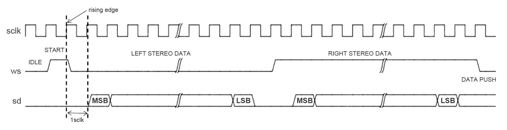
The I2S module of GR551x used the I2S Philips standard. For instance, when WS is low, the word being transferred is left stereo data; when WS is high, the word being transferred is right stereo data. For standard I2S formats, the MSB of a word is sent one SCLK cycle after a WS change. Serial data sent by the transmitter can be synchronized with either the negative edge or positive edge of the SCLK signal. However, the receiver must latch the serial data on the rising edge of SCLK.
图 47 illustrates an example I2S transfer in which I2S Controller is a slave. The IDLE state of WS line is 0. Whenever the WS line makes a transition to 1, it means that after the next transition (0->1), the data starts being received. Therefore, the I2S Controller slave treats the transfer as a START condition. When the stereo data is completely latched (signaled by Word Select Line going 0 again, also treated as start of new data frame), the data is pushed into the internal FIFO.
Sampling and CLK
As the frequency of SCLK up to 3072 kHz, the number of SCLK cycles for which the word select the WS line of I2S can configured as 16 SCLK cycles, 24 SCLK cycles or 32 SCLK cycles (configure SCLK_CFG.WS_SCLK). If select the 16 SCLK cycles, the sample rate is up to 96 kHz. The calculation formula is as follows:
- sample rate = frequency of SCLK / (2 X Sampling depth (16,24 or 32))
- sample rate = frequency of WS(LRCK)
The I2S module can be used as master or slave. The instance of master mode is I2S_M and the instance of slave mode is I2S_S. When configured as a master, I2S controller initializes the WS signal and supplies the clock gating and clock enabling signals. Otherwise, when configured as a slave, I2S controller responds to externally generated SCLK and WS signals. Working in master mode, the I2S Clock Generation must be enabled by setting the Clock Enable Register (CLK_EN) bit0 to ‘1’.
If the I2S module is used as master, the I2S Clock Configure Register (CLK_CFG) should be properly configured. The value of CLK_CFG register bit0 – bit11 (DIV) is decided by the sample rate, sampling depth (16, 24 or 32) and clock divider source (bit18).
For example, the CLK_CFG bit18 is ‘1’ (32 MHz) and the sample rate is 48 kHz, the calculation formula is as follows:
div_TEMP0 = 32MHz *10       / (2 X Sampling Depth X Sample Rate)
if ((div_TEMP0%10) >= 5) /****** Rounding****/
{
    div_TEMP1 = div_TEMP0/10+1;
}
else
{
    div_TEMP1 = div_TEMP0/10;
}
if (div_TEMP1 >= 2)
{
    DIV = div_TEMP1 – 2;
}
else
{
    DIV = 0;
}
| Common Configurations | 32 MHz | 96 MHz | ||||||
|---|---|---|---|---|---|---|---|---|
| Sample Rate (k) | Bits (Left + Right) | Desired Bit Clock (kHz) | Desired Divider (Value) | Actual Divider (Value) (CLK_CFG.DIV) | Actual Word Size (SCLK_CFG.WS_SCLK) | Desired Divider (Value) | Actual Divider (Value) (CLK_CFG.DIV) | Actual Word Size (SCLK_CFG.WS_SCLK) |
| 8 |
2*8 |
256 |
125 |
125 |
16 |
375 |
375 |
16 |
| 8 |
2*16 |
256 |
125 |
125 |
16 |
375 |
375 |
16 |
| 8 |
2*24 |
384 |
83.333333333 |
83 |
24 |
250 |
250 |
24 |
| 8 |
2*32 |
512 |
62.5 |
63 |
32 |
187.5 |
188 |
32 |
| 48 |
2*8 |
1,536 |
20.83333333 |
21 |
16 |
62.5 |
63 |
16 |
| 48 |
2*16 |
1,536 |
20.83333333 |
21 |
16 |
62.5 |
63 |
16 |
| 48 |
2*24 |
2,304 |
13.88888889 |
14 |
24 |
41.666666667 |
42 |
24 |
| 48 |
2*32 |
3072 |
10.41666667 |
10 |
32 |
31.21951 |
31 |
32 |
| 44.1 |
2*8 |
1,411.2 |
22.67573696 |
23 |
16 |
68.02721088435 |
68 |
16 |
| 44.1 |
2*16 |
1,411.2 |
22.67573696 |
23 |
16 |
68.02721088435 |
68 |
16 |
| 44.1 |
2*24 |
2,116.8 |
15.1171579743 |
15 |
24 |
45.3514739229 |
45 |
24 |
| 44.1 |
2*32 |
2,822.4 |
11.33786848 |
11 |
32 |
34.013605442 |
34 |
32 |
I2S Enable
You must enable the I2S Controller before any data can be received or transmitted into the FIFOs. To enable the component, set the I2S Enable (I2S_EN) bit of the I2S Enable Register (EN) to 1. When you disable the device, it acts as a global disable. To disable I2S Controller, set EN[0] to 0.
After disable, the following events occur:
- TX and RX FIFOs are cleared, and read/write pointers are reset;
- Any data in the process of being transmitted or received is lost;
- All other programmable enables (such as transmitter/receiver block enables and individual TX/RX channel enables) in the component are overridden;
- Generation of master mode clock signals sclk_en, ws_out and sclk_gate are disabled (for instance, they are held low).
When I2S Controller is enabled and configured as a master, the device always starts in the left stereo data cycle (WS = 0), and one SCLK cycle later transitions to the right stereo data cycle (WS = 1). This allows for half a frame of SCLKs to write data to the TX FIFOs and to ensure that any connected slave receivers do not miss the start of the data frame (for instance, the WS 1-to-0 transition) once the SCLK restarts. (When I2S Controller is configured as a slave, WS is externally supplied.) On reset, the EN[0] is set to 0 (disable).
I2S as Transmitter
I2S Master Controller and I2S Slave Controller support 1 I2S transmit (TX) channel. Stereo data pairs (such as, left and right audio data) written to a TX channel by CPU are shifted out serially on the appropriate serial data out line. The shifting is timed with respect to the serial clock (SCLK) and the word select line (WS).
图 48 illustrates the basic usage flow for an I2S Controller when it acts as a transmitter.

I2S as Receiver
I2S Master Controller and I2S Slave Controller support 1 I2S receive (RX) channel. Stereo data pairs (such as, left and right audio data) are received serially from a data input line. These data words are stored in RX FIFOs until they are read by CPU. The receiving is timed with respect to the serial clock (SCLK) and the word select line (WS).
图 49 illustrates the basic usage flow for an I2S Controller when it acts as a receiver.

I2S interrupts
The INT_STAT register, INT_MASK register, RX_OVER register and TX_OVER are provided to manage interrupts. The INT_MASK register is used to enable or disable the TX FIFO Overrun interrupt, TX FIFO Empty interrupt, RX FIFO Overrun interrupt and RX FIFO Data Available interrupt. By reading the INT_STAT register, the triggered interrupt type can be obtained. If the RX FIFO or TX FIFO data overflows, read the RX_OVER register bit0 or TX_OVER register bit0 to clear the RX FIFO Data Overrun interrupt or TX FIFO Data Overrun interrupt.
I2S FIFO and DMA
The I2S module provide four 16-word FIFO, two (I2S_M TX FIFO and I2S_S TX FIFO) for transmit and two (I2S_M RX FIFO and I2S_S RX FIFO) for receive. By configuring the Receive FIFO Configuration Register (RX_FIFO_CFG), you can program the trigger level in the RX FIFO at which the Received Data Available interrupt is generated. By configuring Transmit FIFO Configuration Register (TX_FIFO_CFG), you can program the trigger level in the TX FIFO at which the Empty Threshold Reached Interrupt is generated.
The I2S module supported four DMA channel, one for I2S slave transmit, one for I2S slave receive, one for I2S master transmit and one for I2S master receive. The Receiver Block DMA Register (RX_DMA), Reset Receiver Block DMA Register (RST_RX_DMA), Transmitter Block DMA Register (TX_DMA) and Reset Transmitter Block DMA Register (RST_TX_DMA) are provide to configure these channel.
