Electrical Specifications
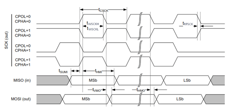
SPIM Electrical Specifications
| Parameter | Description | Min. | Typ. | Max. | Unit |
|---|---|---|---|---|---|
| fSCK |
Clock frequency |
32 |
MHz |
||
| tCSCK |
SCK clock period |
31.25 |
ns |
||
| tRSCK |
SCK rise time, 15 pF loading |
tRF,15pF[1] |
ns |
||
| tFSCK |
SCK fall time, 15 pF loading |
tRF,15pF[1] |
ns |
||
| tWSCKH |
SCK clock high time |
7.625 [2] |
ns |
||
| tWSCKL |
SCK clock low time |
7.625 [2] |
ns |
||
| tSUMI |
Data input setup time (MISO to SCK edge) |
5 |
ns |
||
| tHMI |
Data input hold time (SCK edge to MISO change) |
5 |
ns |
||
| tVMO |
Data output valid time (SCK edge to MOSI valid) |
0 | ns |
||
| tHMO |
MOSI hold time after CLK edge |
20 | ns |
[1] The SCK rise time and the SCK fall time are from 图 42.
[2] The SCK clock high time and the SCK clock low time are calculated by (tCSCK/2)–tRSCK and (tCSCK/2)–tFSCK, respectively.
The SPIM Timing Diagram is as below:
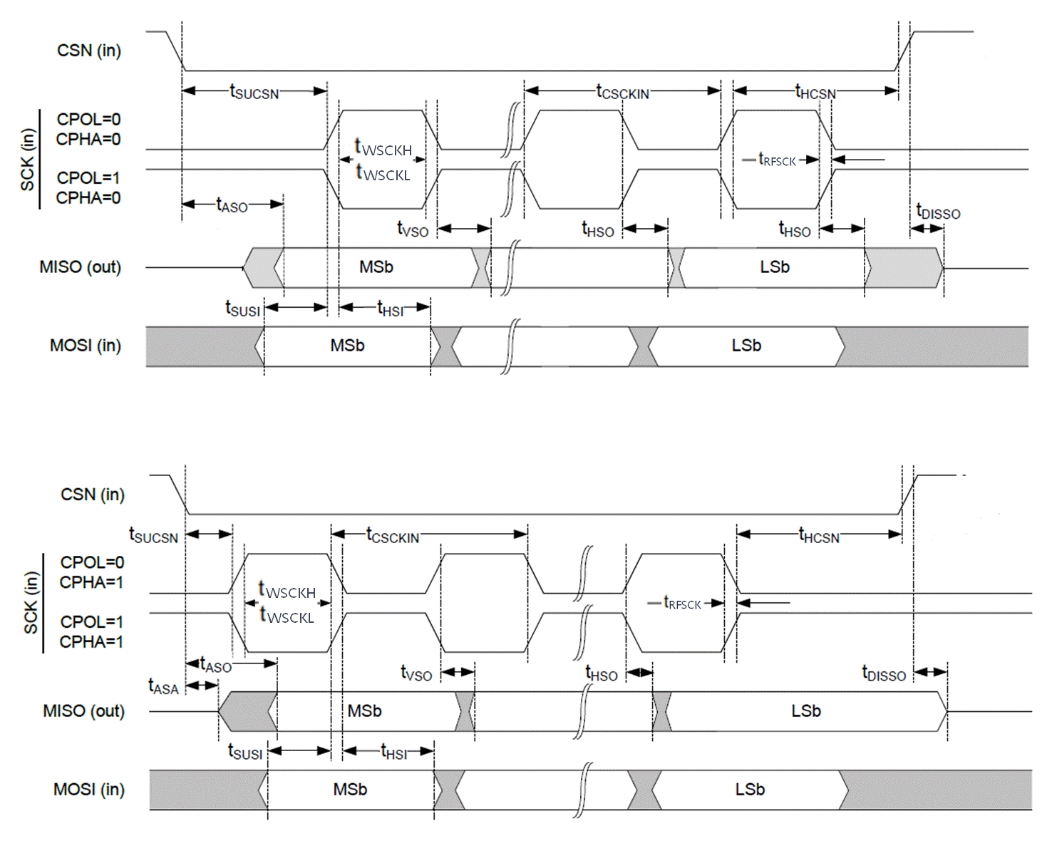
SPIS Electrical Specifications
| Symbol | Description | Min. | Typ. | Max. | Unit |
|---|---|---|---|---|---|
| fSCK |
Clock frequency |
10.67 |
MHz |
||
| tCSCK |
SCK input clock period |
93.7 |
ns |
||
| tRFSCK |
SCK input clock rise/fall time |
22 |
ns |
||
| tWSCKH |
SCK input clock high time |
22 |
ns |
||
| tWSCKL |
SCK input clock low time |
22 |
ns |
||
| tSUCSN |
CSN input setup time |
62.5 |
ns |
||
| tHCSN |
CSN input hold time |
31.25 |
ns |
||
| tASO |
Data output access time (from CSN to MISO valid) |
62.5 |
ns |
||
| tDISSO |
Data output disable time (from CSN to MISO disabled) |
62.5 |
ns |
||
| tVSO |
Data output valid time (from SCK to MISO valid) |
20 |
ns |
||
| tHSO |
Data output hold time (from SCK to MISO change) |
8 |
ns |
||
| tSUSI |
Data input setup time (from MOSI to SCK) |
18 |
ns |
||
| tHSI |
Data input hold time (from SCK to MOSI change) |
0 |
ns |
If SPIS performs RX and TX concurrently, Max bit rate will decrease to 5.33 Mbps.
SPIS Timing Diagram is shown below: