
Hardware Behavior
The SIM interface hardware module supports the physical, data link, and transport layer defined in ETSI TS 131 101.
Physical Layer
The SIM interface hardware module interfaces the UICC with the following ports:
- Clock (CLK)
- Reset (RST)
- Input/Output (I/O)
- UICC presence (PRE)
The detailed electrical required characteristic of the ports can be taken from ETSI TS 131 101.
CLK
The SIM clock is derived from the module clock by dividing it by CLK_CFG.CLK_DIV.
The SIM clock frequency shall be in the range of 1 to 5 MHz, 4 MHz during UICC initialization and 5 MHz during normal operation. The clock division has to be chosen accordingly.
RST
The UICC active low reset pin shall be driven by the SIM interface output, and RST controlled by the register CTRL.ACTION.
I/O
The bidirectional I/O pad on chip top level is implemented as open drain with a recommended pull up to VCC of 20 kΩ. If supported by the UICC the I/O pad can use low impedance drivers to save power.
PRE
UICC card holder often serve a card presence contact. Any card presence change will trigger an interrupt (see STAT.PRESENCE_STAT and STAT.IRQ_PRESENCE).
Power States
The SIM interface module is responsible to execute the cold reset, warm reset, clock stop and the power down sequence. Software triggers power state changes by writing register field CTRL. ACTION.
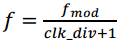
Activation on Cold Reset
The activation sequence and cold reset sequence is shown in 图 52. At first VCC is ramped up. With Ta the clock starts while the reset is still asserted. On Tb the reset is released and the UICC has to start with the ATR within tc.
The I/O pin is not actively driven by the SIM interface during the entire cold reset procedure. The high level is ensured by the pull up resistor. Therefore ta is not implemented in the SIM interface.
tb is hard-coded to 400 clock cycles.
The minimum tc is not checked by the SIM interface module.
The maximum tc is defined by register fields CLK_CFG.ETU_DIV and TIMES_CFG.WAIT_TIME with respect to (6). The reset values are chosen according the specification to receive the ATR without any modifications. CLK_CFG.ETU_DIV is 371 and TIMES.WAITTIME is 107 (see (7)).
If maximum tc is not met by the UICC, interrupt STAT.IRQ_RX_ERR is triggered.
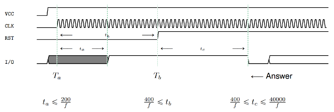
Warm Reset
The warm reset sequence is shown in 图 53.
The warm reset is implemented identical to the cold reset, with Tc = Ta, Td =Tb, td =ta, te = tb and tf =tc.
Due to the fact that the registers CLK_CFG and TIMES_CFG may have changed after the ETU evaluation, the reset values have to be restored by firmware before triggering the warm reset.
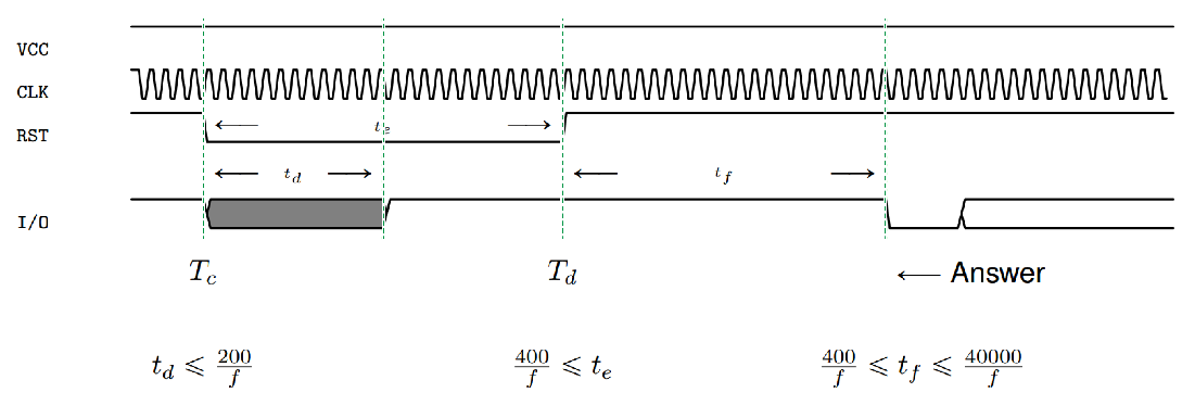
Clock Stop
The clock stop sequence is shown in 图 54.
The times tg and th are ensured by the SIM interface hardware module, with ![]() and
and ![]() .
.
Deactivation
The UICC deactivation sequence is shown in 图 55.
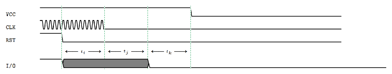
The times ti and tj are ensured by the SIM interface hardware module, with ![]() and
and ![]() .
.
The timing tk depends on the VCC source.
Data Link Layer
Elementary Time Unit (ETU)
The nominal duration of one moment on the electrical circuit I/O is named Elementary Time Unit (ETU).
The ETU shall be equal to F/D clock cycles on the electrical circuit CLK where F and D are the transmission parameters. F is the clock rate conversion integer and D is the baud rate adjustment integer. F, D and f are negotiated during the initialization and setup by firmware. Possible values for F and D are shown in 表 249.
| F | D | F/D |
|---|---|---|
| 372 |
1 |
372 |
| 372 |
2 |
186 |
| 372 |
3 |
124 |
| 372 |
4 |
93 |
| 512 |
1 |
512 |
| 512 |
2 |
256 |
| 512 |
4 |
128 |
| 512 |
8 |
64 |
| 512 |
16 |
32 |
| 512 |
32 |
16 |
| 512 |
64 |
8 |
f is configured as described in CLK.
The chosen ETU has to be written to register field CLK_CFG.ETU_DIV.
Fractional ETU times are not supported.
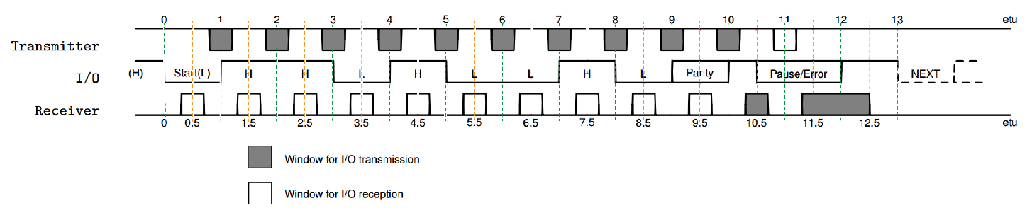
Character Frame
The character transmission timing is shown in 图 56. A character consists of:
- Start Bit
- 8 Data Bits
- Parity Bit
- 2 Stop Bits with error signaling
Error Signal and Character Repetition
- RX
In case of detected parity error during reception, the behavior depends on register field STAT.RX_RETRY_MAX. If the number of retries is not exceeded, the I/O pin is pulled low for one clock cycle to trigger a retransmission. Otherwise or if RETRY_MAX = 0, the received byte is discarded and the reception is aborted with a STAT.IRQ_RETRY_ERR interrupt. The internal retry counter is restarted with every character.
The maximum number of retries during the reception of one byte is displayed in register field STAT.RX_RETRY_MAX and cleared via CTRL.RX_RETYR_MC.
- TX
In case of an error signaling from the receiver, the behavior depends on register field STAT.TX_RETRY_MAX. If the number of retries is not exceeded, the character is retransmitted. Otherwise or if RETRY_MAX = 0, the transmission is aborted with a STAT.IRQ_RETRY_ERR interrupt. The internal retry counter is restarted with every character.
The maximum number of retries during the transmission of one byte is displayed in register field STAT.TX_RETRY_MAX and cleared via CTRL.TX_RETYR_MC.
Guard Time and Wait Time
The guard time specifies the minimum time between the leading edge of two consecutive characters, which has to be taken into account by the transmitter. The wait time specifies the maximum time between the leading edge of two consecutive characters, which has to be monitored by the receiver before issuing a timeout.
The guard time is adjusted by register field TIMES_CFG.GUARD_TIME and respected before transmitting a character. This includes the scenario, when the SIM interface has received a character and starts a transmission afterwards. The minimal guard time is 12. Register field TIMES_CFG.GUARD_TIME values smaller than that are ignored.
The wait time is adjusted by register field TIMES_CFG.WAIT_TIME and respected before aborting a character reception.
Answer to Reset
After a cold or warm reset the UICC answers with the Answer to Reset (ATR). The module receives the ATR and decodes the first byte TS. TS marks the used encoding. If enabled in register field data_cfg.detect_coding the coding is set accordingly in DATA_CFG.CODING. All subsequent bytes are decoded with ISO/IEC 7816-3.
The class selection procedure and the Protocol and Parameter Select (response to the ATR) (PPS) procedure is controlled by firmware. After the PPS procedure, the firmware is responsible to configure the transport protocol, the clock frequency, the I/O mode and the ETU.
Receive and Transmit Buffer
The SIM interface hardware module writes all received data bytes via a Byte DMA to a memory. Transmitted data bytes are read via the same Byte DMA.
Byte DMA
The Byte DMA accesses memory addresses word-wise and interacts with the I/O module on a byte base. In transmitting process, one entire word is read and served byte-wise. Irrelevant bytes are simply ignored. In receiving process, the word is cleared at the beginning and filled byte-wise. After the 4th byte or after receiving the last byte, the entire word is written to the memory.
Address Ranges
Receive and transmit buffer share the same start address (register START_ADDR), which has to be aligned to 4.
The internal word address counting is limited to 18 Bit. Therefore the maximum receive and transmit buffer sizes are limited to 2(18+2) Bytes (1 MB). The buffer shall not cross a 1 MB address boundary.
Receive Buffer
The receive buffer end address is controlled by register RX_END_ADDR and has to be calculated according to (10) for an expected number of bytes NRX.
A done interrupt will be issued after receiving NRX bytes.
If less bytes are received and the wait time is expired, an rx_err interrupt is triggered. The register addr points to the last received byte, which can be used to calculate the number of received bytes nrx.
If more bytes are served by the UICC than expected, an rx_err interrupt is triggered too, but the incoming bytes are ignored and addr stays untouched.
Transmit Buffer
The transmit buffer end address is controlled by register TX_END_ADDR and has to be calculated according to (12) for an expected number of bytes NTX.
DMA Error
A DMA error interrupt dma_err is triggered under the following conditions:
- Invalid address
- Bus slave responses with an error
- Word could not be read within one ETU
- Word could not be written within one character
