
Functional Description
The I2C Controller is made up of an APB slave interface, an I2C interface, and FIFO logic to maintain coherency between the two interfaces as well as DMA and interrupt logics. A simplified block diagram is illustrated in 图 24.

I2C Operation
The I2C is a synchronous serial interface. The SDA line is a bidirectional signal and changes only when the SCL line is low, except for STOP, START, and RESTART conditions. The output drivers are open-drain or open-collector to perform wired-AND functions on the bus. The maximum number of devices on the bus is limited by only the maximum capacitance specification of 400 pF. Data is transmitted in byte packages.
The master is responsible for generating the clock and controlling the transfer of data. The slave is responsible for either transmitting or receiving data to/from the master. The acknowledgement of data is sent by the device that is receiving data, which can be either a master or a slave. The I2C protocol also allows multiple masters to reside on the I2C bus and uses an arbitration procedure to determine the bus ownership.
When a master wants to communicate with a slave, the master transmits a START/RESTART condition that is then followed by the slave’s address and a control bit (R/W) to determine if the master wants to transmit data to or receive data from the slave. The slave then sends an acknowledge (ACK) pulse after the address.
If the master (master-transmitter) is writing to the slave (slave-receiver), the receiver gets one byte of data. This transaction continues until the master terminates the transmission with a STOP condition. If the master is reading from a slave (master-receiver), the slave transmits (slave-transmitter) a byte of data to the master, and the master then acknowledges the transaction with the ACK pulse. This transaction continues until the master terminates the transmission by not acknowledging (NACK) the transaction after the last byte is received, and then the master issues a STOP condition or addresses another slave after issuing a RESTART condition. This behavior is illustrated in 图 25.
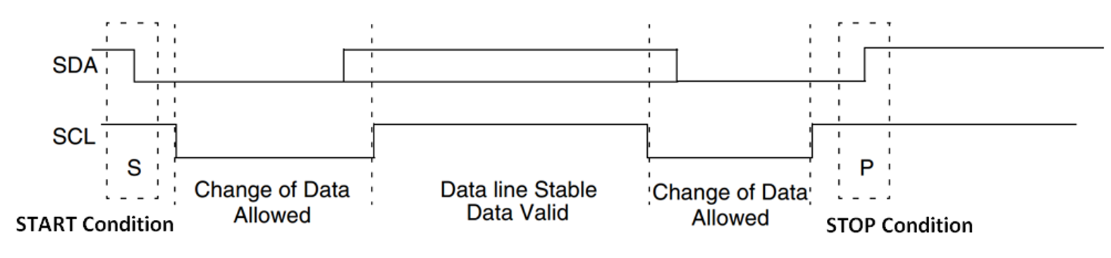
START and STOP Conditions
When I2C operates as a Master, putting data into the transmit FIFO causes the I2C block to generate a START condition on the I2C bus. Writing 1 to IC_DATA_CMD[8] causes the I2C block to generate a STOP condition on the I2C bus; a STOP condition is not issued if this bit is not set, even if the transmit FIFO is empty.
When the bus is idle, both the SCL and SDA signals are pulled high through external pull-up resistors on the bus. When a master wants to start a transmission on the bus, the master issues a START condition. This is defined as a high-to-low transition of the SDA signal while SCL is high. When a master wants to terminate the transmission, the master issues a STOP condition. This is defined as a low-to-high transition of the SDA line while SCL is high. 图 26 shows the timing of the START and STOP conditions. When data is being transmitted on the bus, the SDA line must be stable when the SCL is high.
Addressing Slave
There are two address formats: the 7-bit address format and the 10-bit address format. The I2C block supports mixed read and write combined format transactions in 7-bit or 10-bit addressing modes. The I2C block does not support mixed address and mixed address format, that is, a 7-bit address transaction followed by a 10-bit address transaction or vice versa (combined format transactions).
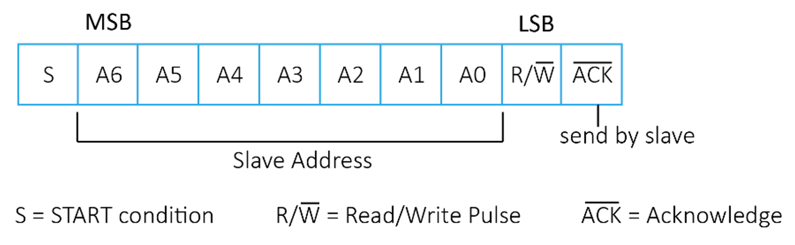
7-bit Address Format
Using the 7-bit address format, the first seven bits (bits 7:1) of the first byte set the slave address and the least significant bit (bit 0) (LSB) is the R/W bit as shown in 图 27. When bit 0 (R/W) is set to 0, the master writes to the slave. When bit 0 (R/W) is set to 1, the master reads from the slave.
10-bit Address Format
Using the 10-bit address format, two bytes are transferred to set the 10-bit address. The transfer of the first byte contains the following bit definition. The first five bits (bits 7:3) notify the slave that this is a 10-bit transfer followed by the next two bits (bits 2:1), which set the slave address (bits 9:8), and the LSB bit (bit 0) is the R/W bit. The second byte transferred sets bits 7:0 of the slave address. 图 28 shows the 10-bit address format.
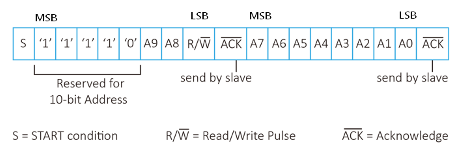
表 85 defines the special purpose and reserved first byte addresses.
| Slave Address | R/W Bit | Description |
|---|---|---|
| 0000 000 | 0 | General Call Address. DW_apb_i2c places the data in the receive buffer and issues a General Call interrupt. |
| 0000 000 | 1 | START byte |
| 0000 001 | X | CBUS address. I2C ignores these accesses. |
| 0000 010 | X | Reserved |
| 0000 010 | X | Reserved |
| 0000 011 | X | High-speed master code |
| 1111 1XX | X | Reserved |
| 1111 0XX | X | 10-bit slave addressing |
| 0001 000 | X | SMBus Host |
| 0001 100 | X | SMBus Alert Response Address |
| 1100 001 | X | SMBus Device Default Address |
Transmitting and Receiving
A master can initiate data transmission and reception to/from the bus, acting as either a master-transmitter or master-receiver. A slave responds to requests from the master to either transmit data or receive data to/from the bus, acting as either a slave-transmitter or slave-receiver, respectively.
Master-Transmitter and Slave-Receiver
All data is transmitted in byte format, with no limit on the number of bytes transferred per data transfer. After the master sends the address and R/W bit or the master transmits a byte of data to the slave, the slave-receiver must respond with the ACK signal. When a slave-receiver does not respond with an ACK pulse, the master aborts the transfer by issuing a STOP condition. The slave must leave the SDA line high so that the master can abort the transfer.
If the master-transmitter is transmitting data as shown in 图 29, the slave-receiver responds to the master-transmitter with an ACK pulse after every data byte is received.
Master-Receiver and Slave-Transmitter
If the master is receiving data as shown in 图 30, then the master responds to the slave-transmitter with an ACK pulse after a byte of data has been received, except for the last byte. This is the way the master-receiver notifies the slave-transmitter that this is the last byte. The slave-transmitter relinquishes the SDA line after detecting the No Acknowledge (NACK) so that the master can issue a STOP condition.

START BYTE Transfer
The START BYTE transfer protocol is set up for systems that do not have an on-board dedicated I2C hardware module. When the I2C block is addressed as a slave, it always samples the I2C bus at the highest speed supported so that it never requires a START BYTE transfer. However, when the I2C block is a master, it supports the generation of START BYTE transfers that a slave device might require at the beginning of every transfer.
This protocol consists of seven zeros being transmitted followed by a one, as illustrated in 图 31. This allows the processor that is polling the bus to under-sample the address phase until 0 is detected. Once the microcontroller detects a 0, it switches from the under sampling rate to the correct rate of the master.
The START BYTE procedure is as follows:
- Master generates a START condition.
- Master transmits the START byte (0000 0001).
- Master transmits the ACK clock pulse. (Present only to conform with the byte handling format used on the bus)
- No slave sets the ACK signal to 0.
- Master generates a RESTART condition.
A hardware receiver does not respond to the START BYTE because it is a reserved address and resets after the RESTART condition is generated.
