Electrical Specifications
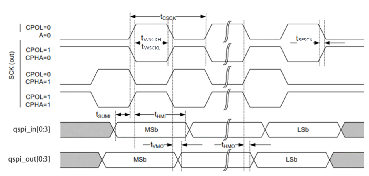
QSPI Electrical Specifications
| Parameter | Description | Min. | Typ. | Max. | Units |
|---|---|---|---|---|---|
| fSCK | Clock frequency | 32 | MHz | ||
| tCSCK | SCK clock period | 31.25 | ns | ||
| tRSCK | SCK rise time, 15 pF loading | tRF,15pF[1] | ns | ||
| tFSCK | SCK fall time, 15 pF loading | tRF,15pF[1] | ns | ||
| tWSCKH | SCK clock high time | 7.625[2] | ns | ||
| tWSCKL | SCK clock low time | 7.625[2] | ns | ||
| tSUMI | Data input setup time (MISO to SCK edge) | 0 | ns | ||
| tHMI | Data input hold time (SCK edge to MISO change) | 8 | ns | ||
| tVMO | Data output valid time (SCK edge to MOSI valid) | 0 | ns | ||
| tHMO | MOSI hold time after CLK edge | 20 | ns |
[1] The SCK rise time and the SCK fall time are from 图 45.
[2] The SCK clock high time and the SCK clock low time are calculated by (tCSCK/2)–tRSCK and (tCSCK/2)–tFSCK, respectively.
The QSPI Timing Diagram is as below: